

Semiconductor device with protection element disposed around a formation region of a transistor
a technology of protection element and formation region, which is applied in the direction of semiconductor/solid-state device details, diodes, transistors, etc., can solve the problems of surge protection element around the pad not being able to cope, uneven breakdown of chips, and inability to absorb surge protection elements, so as to reduce manufacturing costs of semiconductor devices, prevent current concentration, and improve current capacity of protection elements
- Summary
- Abstract
- Description
- Claims
- Application Information
AI Technical Summary
Benefits of technology
Problems solved by technology
Method used
Image

Examples
first embodiment
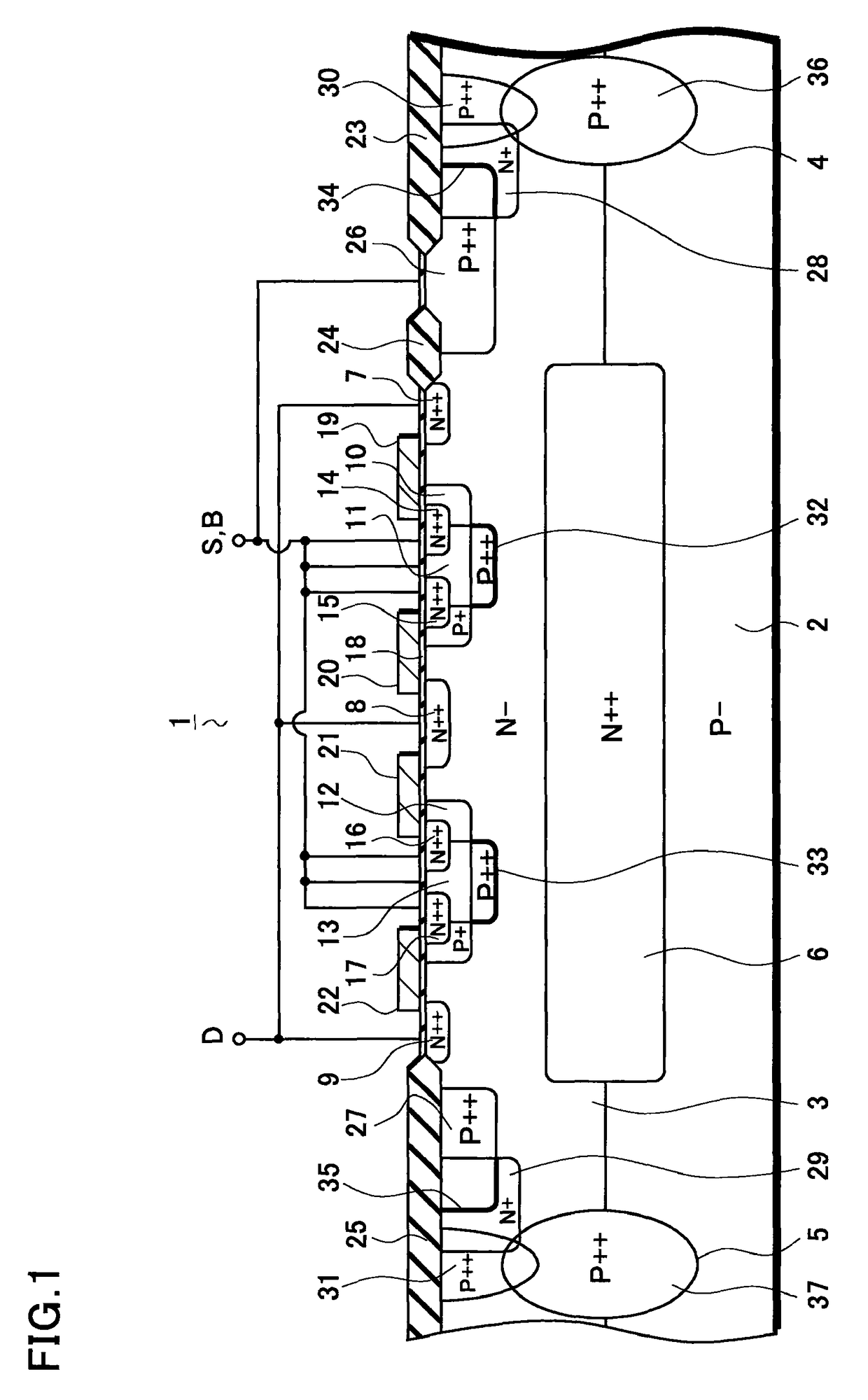
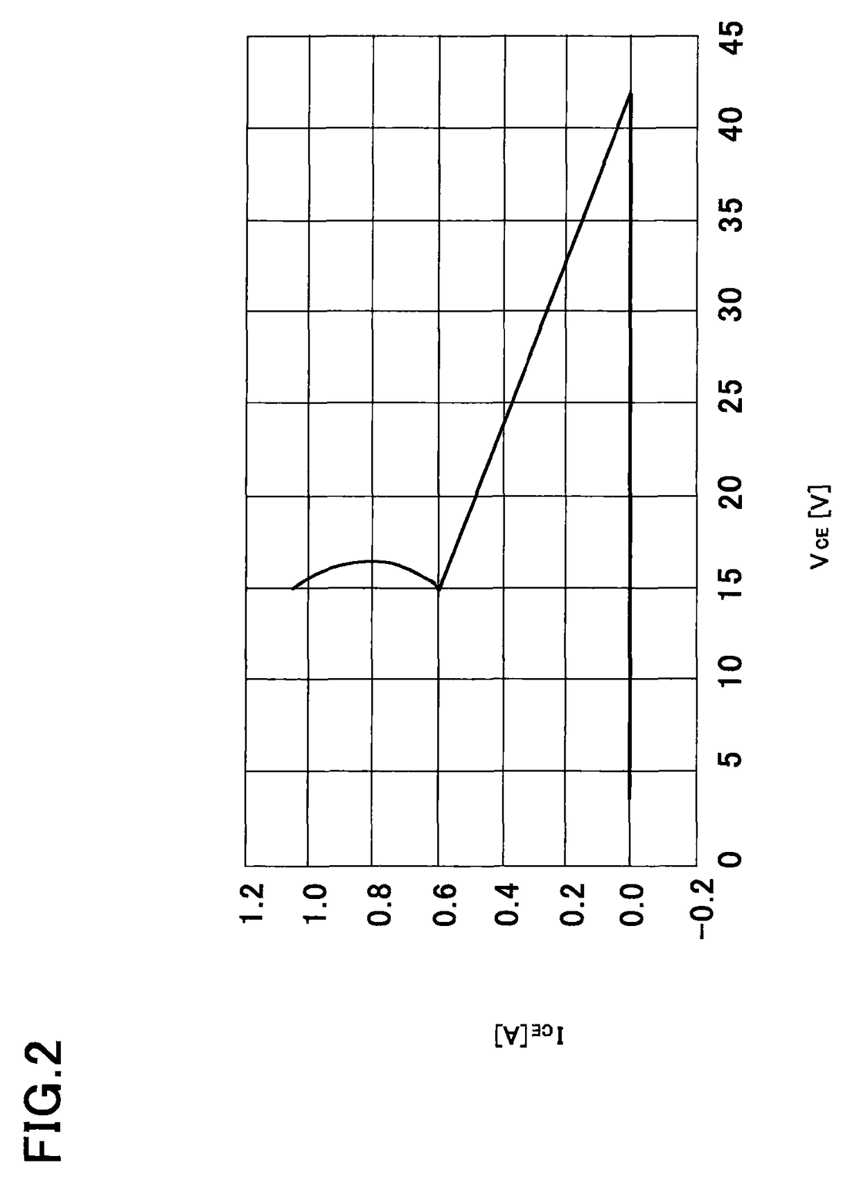
[0035]With reference to FIGS. 1 and 2, a semiconductor device according to the present invention will be described in detail below. FIG. 1 is a cross-sectional view for describing the semiconductor device according to this embodiment. FIG. 2 is a graph for describing characteristics of a protection element in this embodiment.
[0036]As shown in FIG. 1, an N-channel MOS transistor 1 mainly includes a P type single crystal silicon substrate 2, an N type epitaxial layer 3, isolation regions 4 and 5, an N type buried diffusion layer 6, N type diffusion layers 7 to 9 used as drain regions, P type diffusion layers 10 to 13 used as back gate regions, N type diffusion layers 14 to 17 used as source regions, a gate oxide film 18, and gate electrodes 19 to 22.
[0037]The N type epitaxial layer 3 is formed on the P type single crystal silicon substrate 2. Note that, although one epitaxial layer 3 is formed on the substrate 2 in this embodiment, the present invention is not limited to this case. Fo...
second embodiment
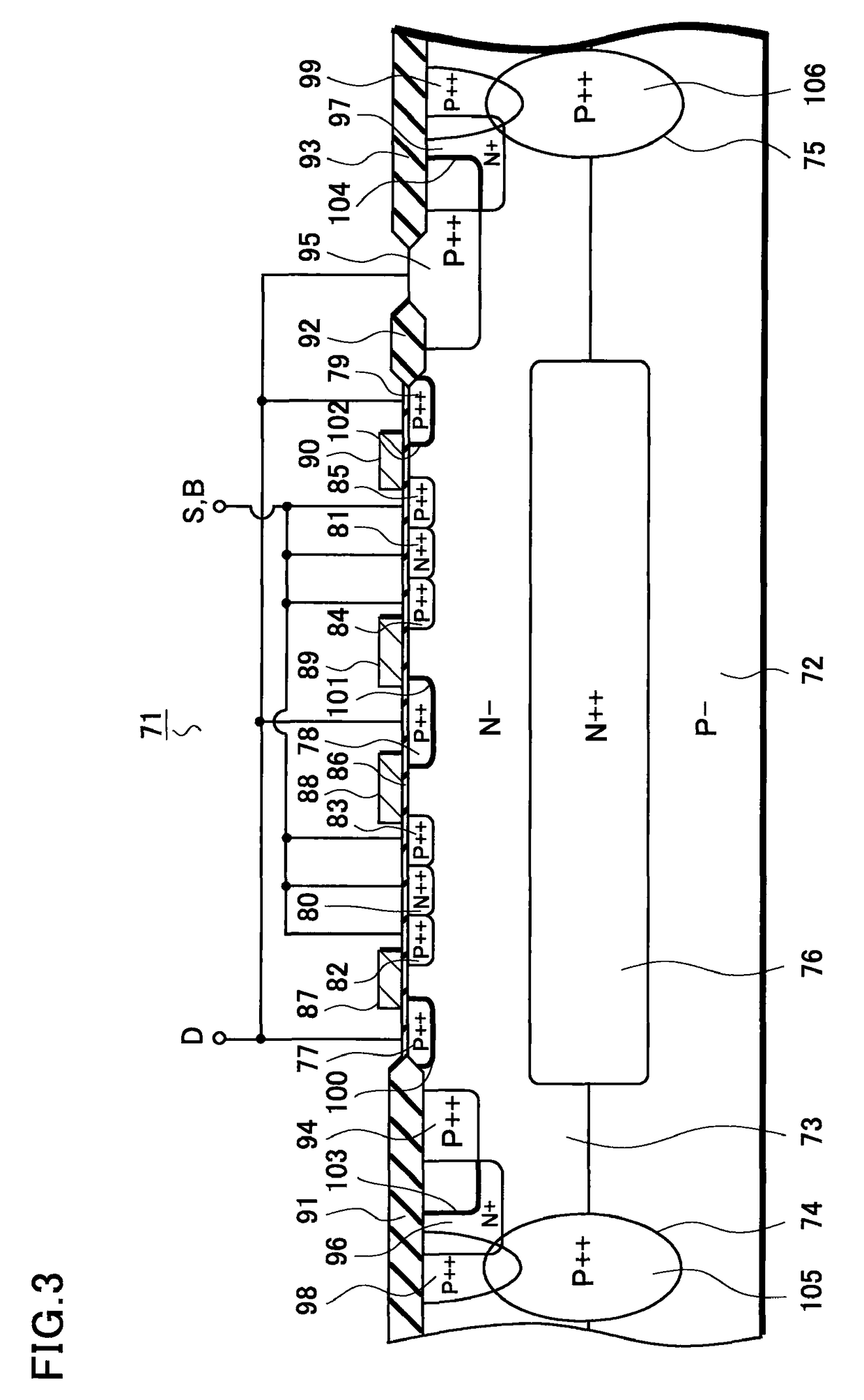
[0071]Next, with reference to FIG. 3, a semiconductor device according to the present invention will be described in detail. FIG. 3 is a cross-sectional view for explaining the semiconductor device according to this embodiment.
[0072]As shown in FIG. 3, a P-channel MOS transistor 71 mainly includes a P type single crystal silicon substrate 72, an N type epitaxial layer 73, isolation regions 74 and 75, an N type buried diffusion layer 76, P type diffusion layers 77 to 79 used as drain regions, N type diffusion layers 80 and 81 used as back gate regions, P type diffusion layers 82 to 85 used as source regions, a gate oxide film 86, and gate electrodes 87 to 90.
[0073]The N type epitaxial layer 73 is formed on the P type single crystal silicon substrate 72. Note that, although one epitaxial layer 73 is formed on the substrate 72 in this embodiment, the present invention is not limited to this case. For example, the substrate is stacked with a plurality of epitaxial layers.
[0074]Each of t...
PUM
 Abstract
Description
Claims
Application Information