Method and apparatus for producing gallium arsenide and silicon composites and devices incorporating same

a gallium arsenide and composite technology, applied in the direction of crystal growth process, polycrystalline material growth, radiofrequency control device, etc., can solve the problems of difficult layering of gallium arsenide and silicon composites, difficult to layer them together, and rather expensive gaas films or grown as gaas wafers,

Inactive Publication Date: 2011-04-12
BOWLING GREEN STATE UNIV
View PDF1 Cites 1 Cited by
  • Summary
  • Abstract
  • Description
  • Claims
  • Application Information

AI Technical Summary

Benefits of technology

[0032]The invention also includes memory/logic/multiplexer devices including a layered article of gallium arsenide upon a silicon substrate. A memory device can store digitized information over a long period of time. The stored information can be retrieved, deleted or overwritten by newer information. Normally, these structures are achieved with field effect transistors, and this may be done with the GaAs/Si multiplexer by charging a capacita

Problems solved by technology

In general, in order to achieve high-quality epitaxial growth, GaAs films or grown as GaAs wafers, which are rather expensive.
One of the difficulties in combining these two materials is that it has been difficult to layer them together so as to achieve a stoichiometric combination of the two species.
However, it s

Method used


Image

  • Method and apparatus for producing gallium arsenide and silicon composites and devices incorporating same
  • Method and apparatus for producing gallium arsenide and silicon composites and devices incorporating same
  • Method and apparatus for producing gallium arsenide and silicon composites and devices incorporating same

Examples


Embodiment Construction

)

[0065]In accordance with the foregoing summary, the following is a more detailed description of the preferred embodiments of some of the present inventions which are considered to be the best mode thereof.

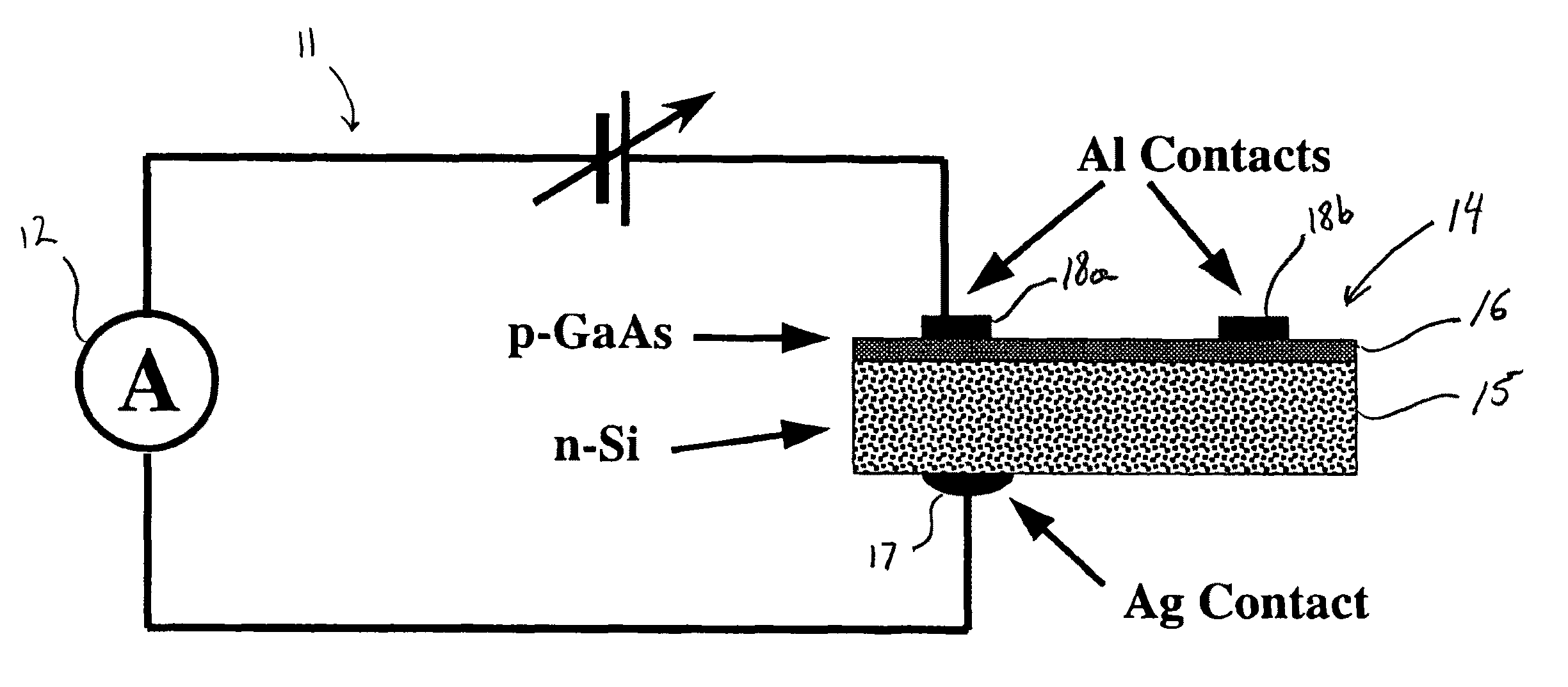
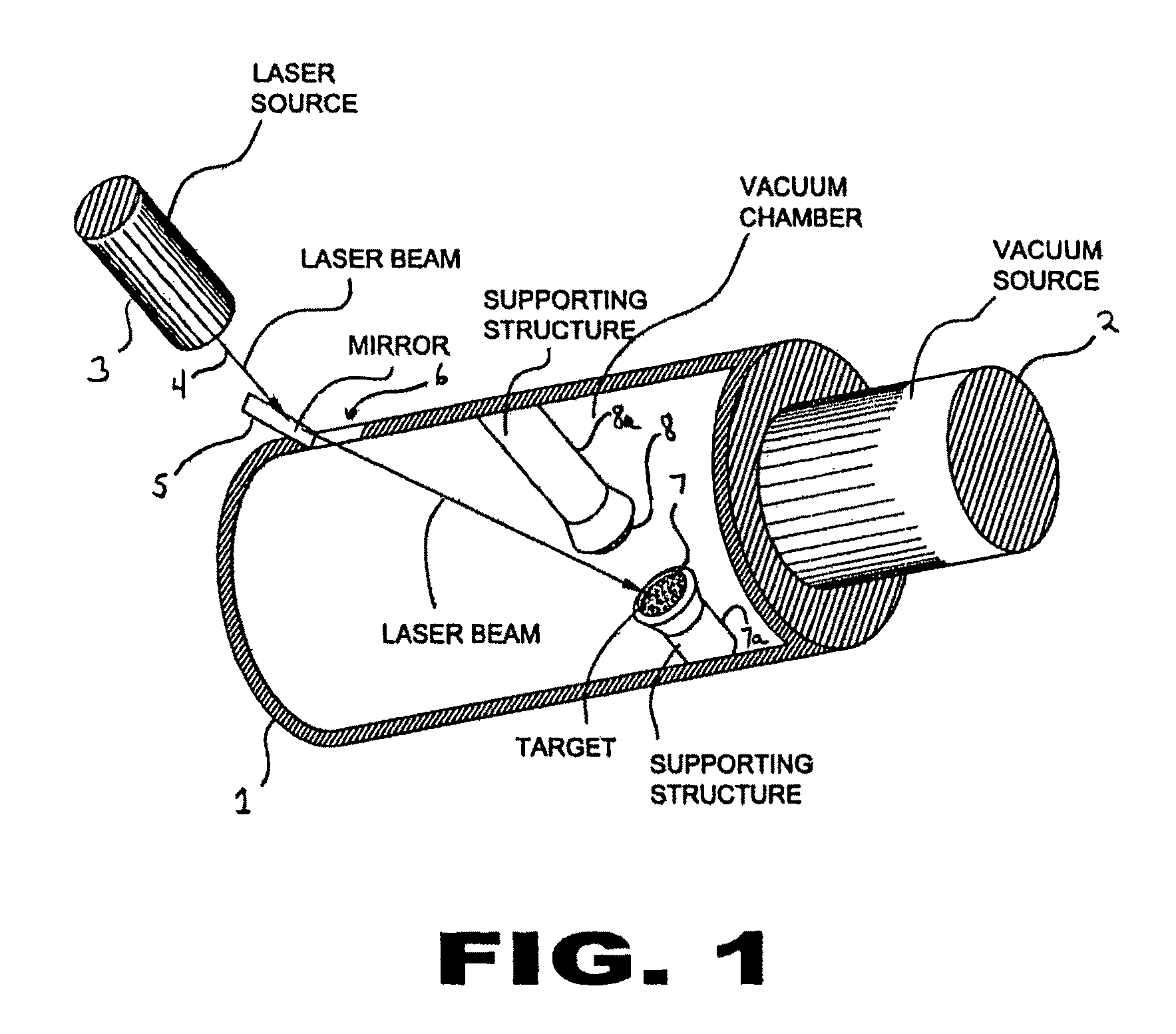
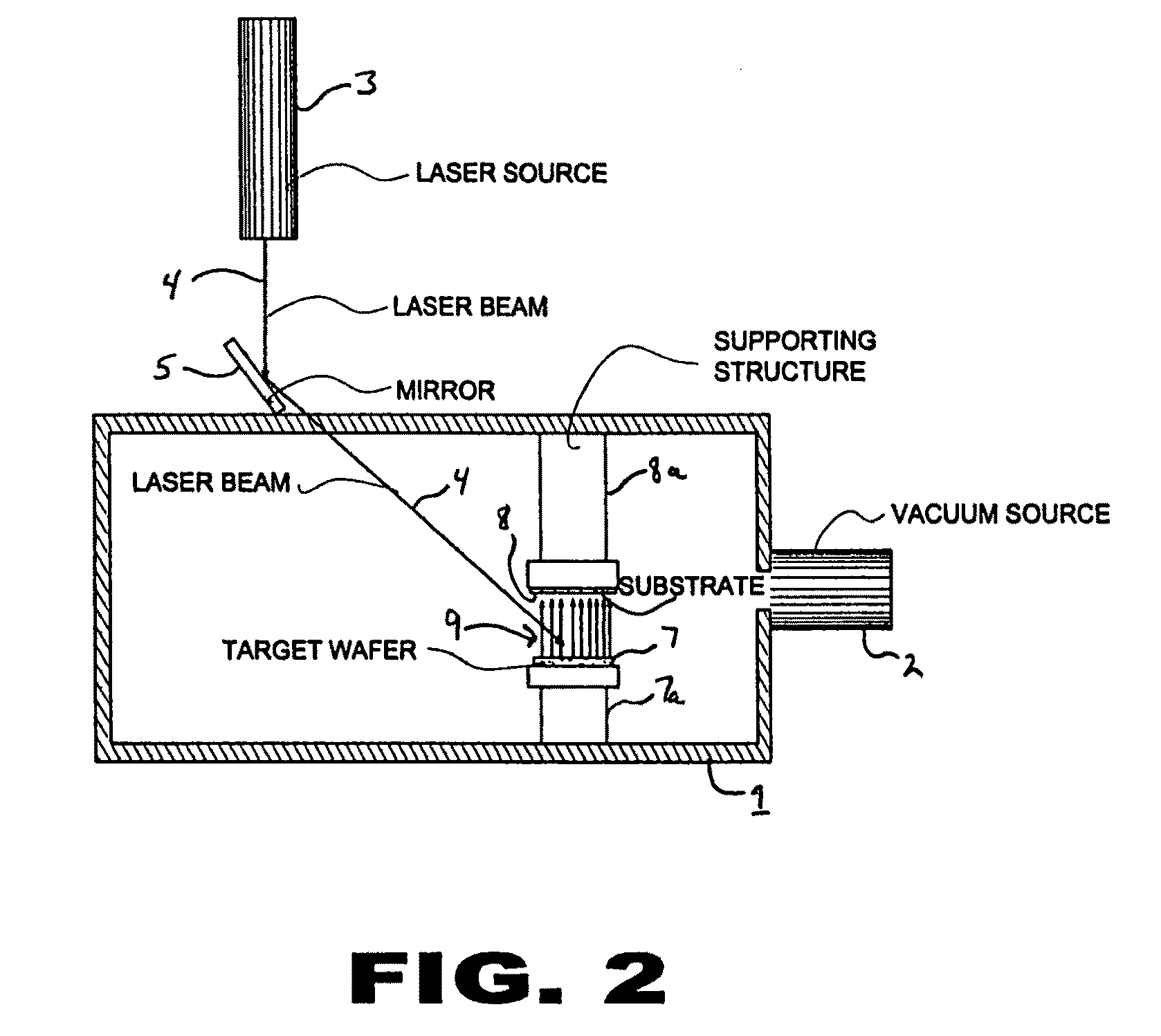
[0066]With respect to the preferred embodiment of the deposition of the present invention, the GaAs ablation used the 532 nm emission of a Nd:YAG laser (10 Hz repetition rate; 6 ns pulse) with a fluence of 0.79-0.84 J / cm2. The laser spor size was about 1.8 mm×2.5 mm (elliptical). The thicknesses of the films were approximately 0.5 μm. During the deposition of about one hour in duration, the substrate was not heated and the ambient pressure was kept at about 10-6-10-7 torr. X-ray analysis showed that the films contain crystallites and by means of an atomic force microscope (AFM), it is demonstrated that the film surfaces are fairly smooth. Using a monochromatic light source and by means of electrical contacts on the top and the rear of the sample, we measured the photocurrent (PC) ...


PUM


Abstract

The present invention includes methods for producing GaAs/Si composites, GaAs/Si composites, apparatus for preparing GaAs/Si composites, and a variety of electronic and photoelectric circuits and devices incorporating GaAs/Si composites of the present invention.

Description

RELATED APPLICATION DATA[0001]This application is a divisional of U.S. application Ser. No. 10 / 773,886 filed Feb. 6, 2004 now abandoned, which is incorporated herein by reference.BACKGROUND OF THE INVENTION[0002]The present invention relates to a method and apparatus for producing layered composites of gallium arsenide and silicon, layered articles produced there by and devices produced therefrom.[0003]The III-V compound semiconductor GaAs has a rapidly growing impact on electronic circuits and optoelectronic devices. Thus the control preparation of GaAs films of appreciable technological interest. In general, in order to achieve high-quality epitaxial growth, GaAs films or grown as GaAs wafers, which are rather expensive. On the other in the most important achieve semiconductor silicon is nonstandard substrate for high-quality of gallium arsenide preparations. The GaAs devices prepared on silicon substrates, however, would be considered to increase the flexibility of optoelectronic...

Claims


Application Information

Patent Timeline
IPC IPC(8): H01L31/062
CPCC30B25/105C30B29/42H01L31/1852H01L31/109Y02E10/544
Inventor ULLRICH, BRUNOERLACHER, ARTUR
Owner BOWLING GREEN STATE UNIV
Why Eureka
Try Eureka