
Poly etch without separate oxide decap

a polysilicon layer and oxide decapping technology, applied in the direction of microstructural devices, solid-state devices, microstructural technology, etc., can solve the problems of increasing the size of mem devices, increasing the cost and power consumption of many cases, and slow plasma etching process

Inactive Publication Date: 2011-04-19
MICRON TECH INC
View PDF89 Cites 2 Cited by
  • Summary
  • Abstract
  • Description
  • Claims
  • Application Information

AI Technical Summary

Problems solved by technology

Reducing the size of MEM devices increases their utility and decreases their price and power consumption in many cases.
However, plasma etch processes are slow, require substantial expensive equipment, and may have problems with what may be known as etch selectivity ratios.
Wet etching is simple and inexpensive, but there is an issue with the etch uniformity, both in terms of across the single wafer variations, and in lot to lot variations over time.
Wet chemical etches that have high poly etch rates and high etch selectivity over underlying oxides may be non uniform since the etching of the poly can not begin until the native oxide, which may be call a cap oxide, is etched (or decapped).
Since the thickness of the oxide cap is a variable that depends at least in part on how long the poly layer has been exposed, and the storage conditions, then the amount of time it takes to decap the poly layer before etching begins may result in non-uniform etching.
However, the wafers must be washed in deionized water (DI water) and dried prior to going into the poly etch bath, and such a washing procedure may cause sufficient native oxide to regrow to again inhibit the initiation of the poly etch.
Further, the variations in the amount of time that pass between the end of the decap process and the beginning of the poly etch may again result in lot to lot variations in the amount of poly etched.
Yet further, the need to have two different wet chemical baths and the increase in production time and cost make this solution less than optimal.
There may also be an operator safety issue in having an acid bath in the same general vicinity as the typically caustic poly etch bath, since acids and bases should not be mixed without safety precautions.

Method used


Image

  • Poly etch without separate oxide decap
  • Poly etch without separate oxide decap
  • Poly etch without separate oxide decap

Examples


Embodiment Construction

The following detailed description refers to the accompanying drawings that show, by way of illustration, specific aspects and embodiments in which the present invention may be practiced. These embodiments are described in sufficient detail to enable those skilled in the art to practice the present invention. Other embodiments may be utilized and structural, logical, and electrical changes may be made without departing from the scope of the present invention. The various embodiments are not necessarily mutually exclusive, as some embodiments can be combined with one or more other embodiments to form new embodiments.

The terms wafer and substrate used in the following description include any structure having an exposed surface with which to form an integrated circuit (IC) structure or a micro electro-mechanical (MEM) structure. The term substrate is understood to include semiconductor wafers. The term substrate is also used to refer to semiconductor structures during processing, and m...


PUM

PropertyMeasurementUnit
Temperatureaaaaaaaaaa

Abstract

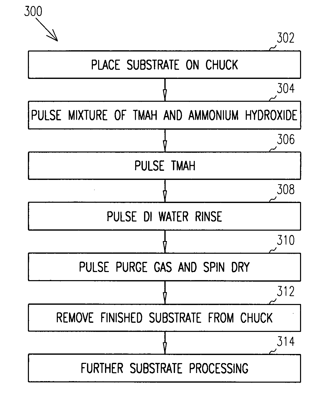
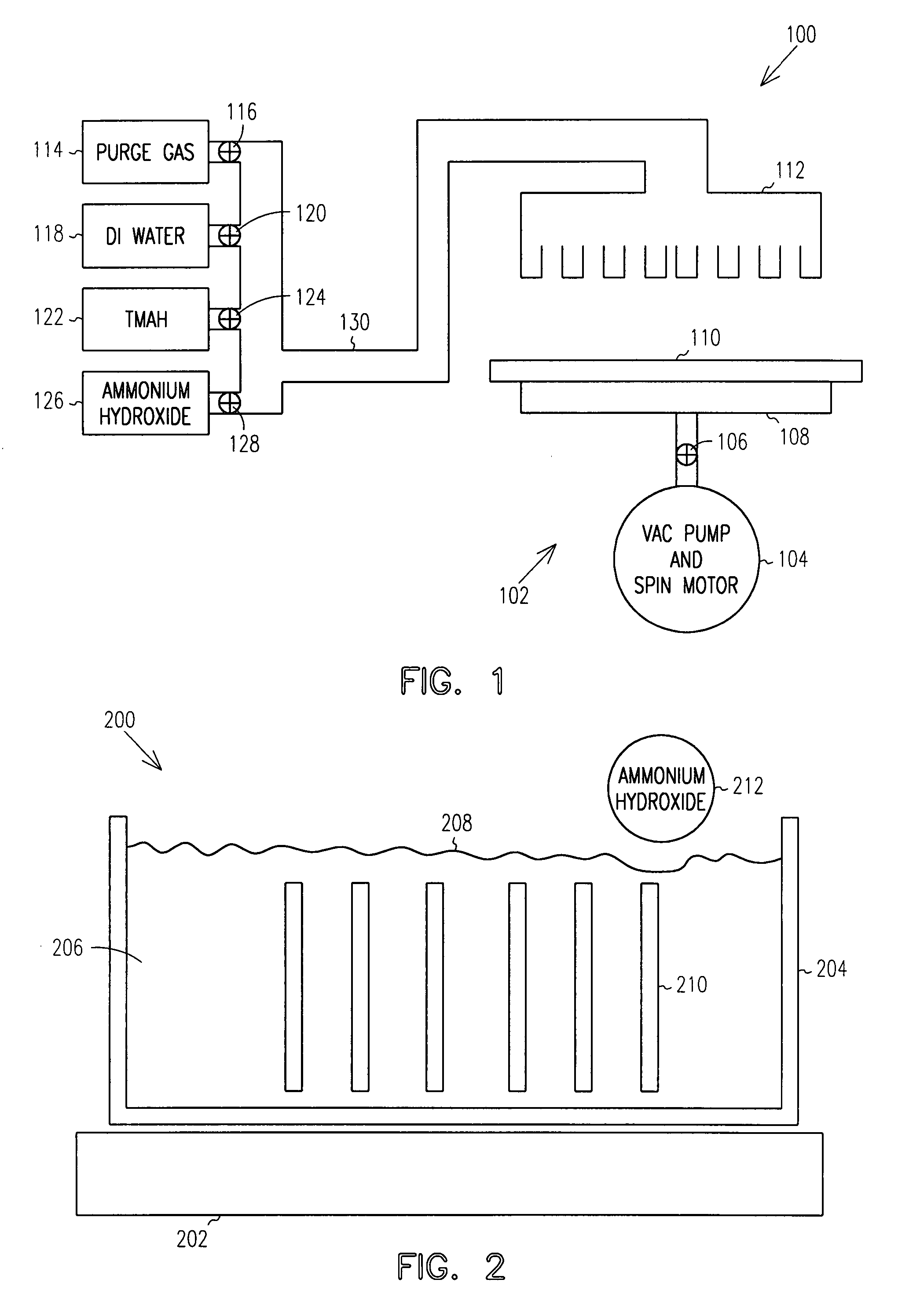
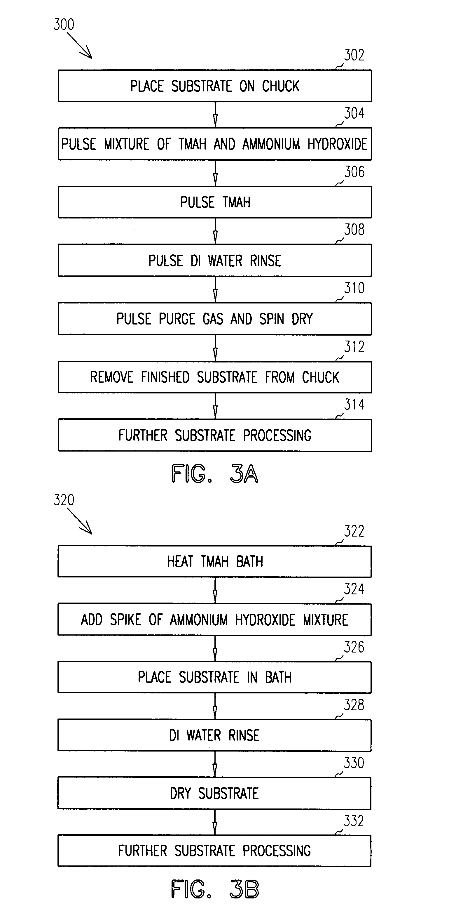
The use of an ammonium hydroxide spike to a hot tetra methyl ammonium hydroxide (TMAH) solution to form an insitu poly oxide decapping step in a polysilicon (poly) etch process, results in a single step rapid poly etch process having uniform etch initiation and a high etch selectivity, that may be used in manufacturing a variety of electronic devices such as integrated circuits (ICs) and micro electro-mechanical (MEM) devices. The etching solution is formed by adding 35% ammonium hydroxide solution to a hot 12.5% TMAH solution at about 70° C. at a rate of 1% by volume, every hour. Such an etch solution and method provides a simple, inexpensive, single step self initiating poly etch that has etch stop ratios of over 200 to 1 over underlying insulator layers and TiN layers.

Description

TECHNICAL FIELDThis application relates generally to semiconductor devices and device fabrication and, more particularly, to etching polysilicon layers without a separate oxide decapping procedure.BACKGROUNDThe semiconductor device industry has a market driven need to reduce the size of devices such as transistors, capacitors and electrically conductive interconnects in order to produce smaller integrated circuit devices (ICs). Smaller ICs result in improved operational speed and clock rate, and reduced power requirements in both the standby and operational modes. Smaller ICs need thinner dielectric layers, thinner diffusion layers and more closely spaced conductive interconnect layers, such as doped polycrystalline silicon (poly). Producing these closely spaced (finer pitch) poly lines requires improved poly etching techniques. Micro electro-mechanical (MEM) devices may use etched poly patterns as a portion of the device. Reducing the size of MEM devices increases their utility and...

Claims


Application Information

Patent Timeline
IPC IPC(8): B44C1/22H01L21/302
CPCB81C1/00595H01L27/1052H01L21/76838H01L21/32134H10B99/00
Inventor SHEA, KEVIN
Owner MICRON TECH INC
Learn More