
Average power efficiency enhancement and linearity improvement of microwave power amplifiers
a technology of power amplifiers and bias networks, which is applied in the direction of amplifiers, amplifiers with semiconductor devices only, amplifiers with semiconductor devices, etc., can solve the problems of in-band distortion and out-of-band emission of power amplifiers, power amplifiers consume a significant amount of power, and the effect of increasing the power consumption
- Summary
- Abstract
- Description
- Claims
- Application Information
AI Technical Summary
Benefits of technology
Problems solved by technology
Method used
Image

Examples
Embodiment Construction
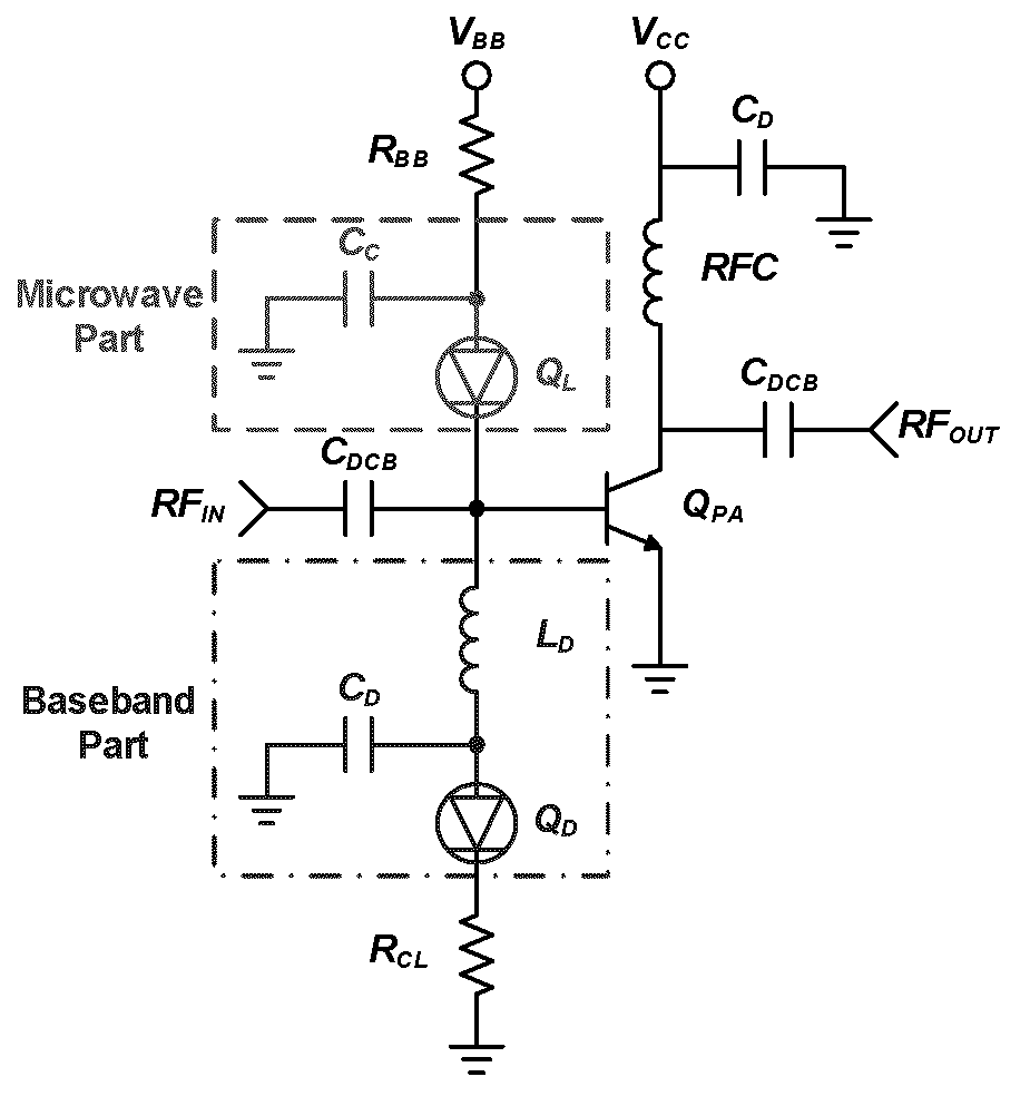
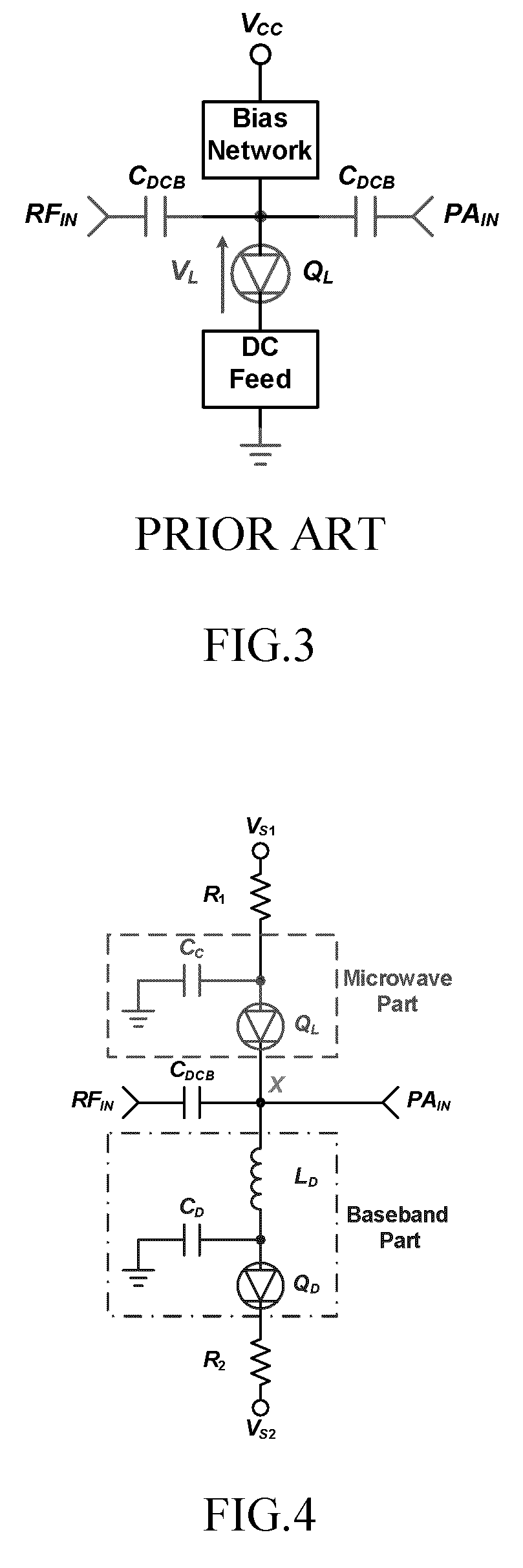
[0037]FIG. 4 shows the general structure of an embodiment of the self-adaptive bias network. The network is connected at a node located between the port of input RF signal (RFIN) and the input port of the microwave transistor (PAIN). The network can be divided into two parts: baseband and microwave parts. The baseband part includes an RF choking inductor LD, a decoupling capacitor CD and a forward-biased diode QD. LD is used to isolate the RF signals, bypass low frequency components and provide a DC path to QD. CD is used to bypass all AC signals, including the leakage of RF signals and the low frequency intermodulation products, to ground. QD acts as a voltage stabilizer and a current source. The microwave part includes a forward-biased diode QL and a coupling capacitor CC. QL acts as a rectifier and a predistorter. CC serves to control the coupling effect of the input RF signals to QL. It should also be understood that the forward-based diodes QD and QL can be implemented either b...
PUM
 Abstract
Description
Claims
Application Information