Gallium nitride traveling wave structures

a gallium nitride and traveling wave technology, applied in the direction of solid-state devices, amplifiers with transit-time effect, multi-port active networks, etc., can solve the problems of limited power density and bandwidth of gaas devices, few devices can even operate at high power above 50 ghz, and prior art structures providing amplification at high frequencies have proved unsatisfactory, etc., to achieve wide bandwidth and high power density

Inactive Publication Date: 2011-05-03
LOCKHEED MARTIN CORP +1
View PDF5 Cites 17 Cited by
  • Summary
  • Abstract
  • Description
  • Claims
  • Application Information

AI Technical Summary

Problems solved by technology

Prior art structures providing amplification at high frequencies have proven unsatisfactory and very few devices can even operate at high power above 50 GHz.
However, operation of such GaAs devices is limited in power density and bandwidth.
In prior art devices the capacitance between the gate and source electrodes (Cgs) of such FETs is very high and the power is limited by the voltage breakdown of the devices.

Method used


Image

  • Gallium nitride traveling wave structures
  • Gallium nitride traveling wave structures
  • Gallium nitride traveling wave structures

Examples


Embodiment Construction

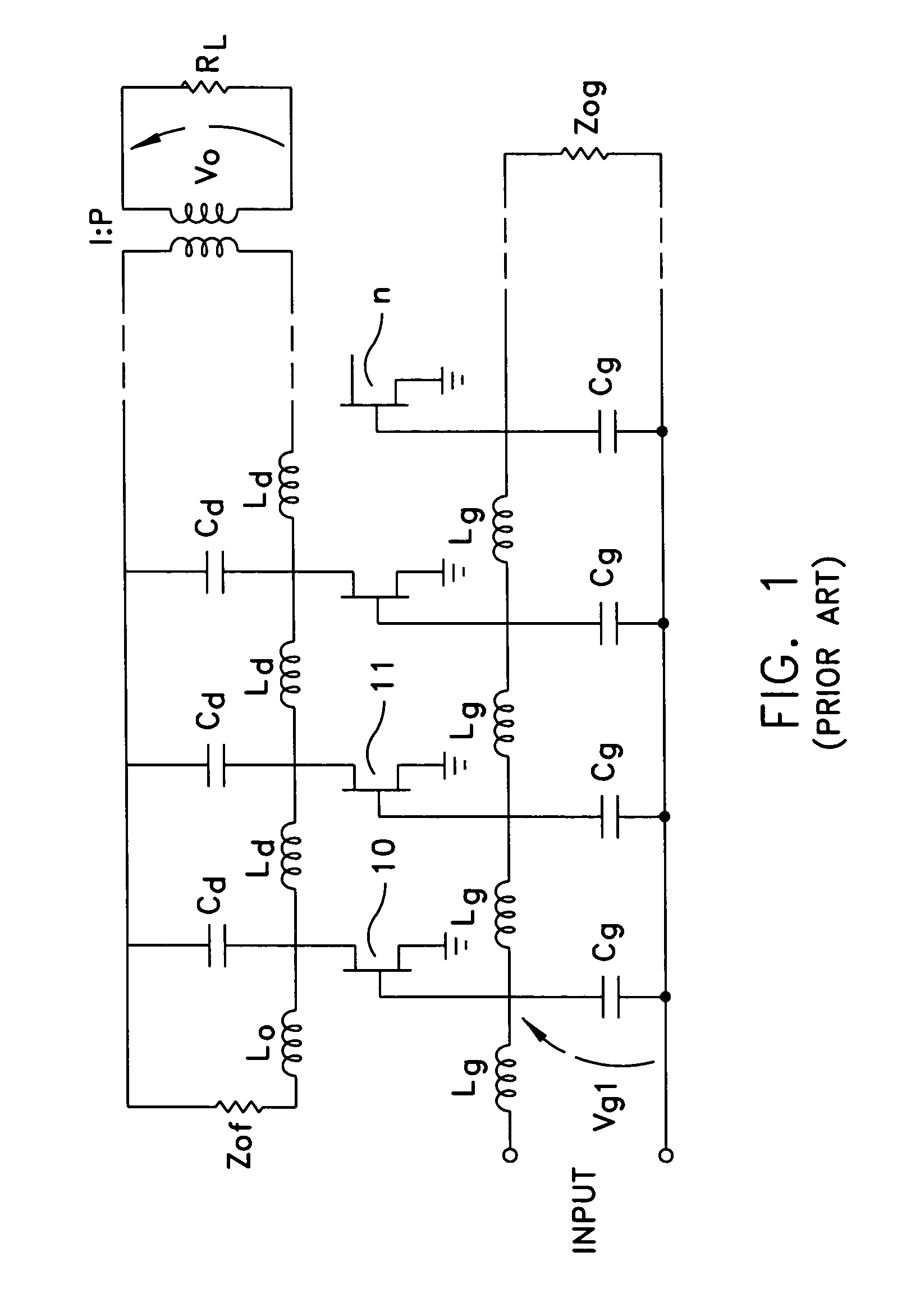
[0019]Referring to FIG. 1, there is shown a traveling wave FET distributed amplifier according to the prior art. The structure shown in FIG. 1 is depicted in FIG. 4 of U.S. Pat. No. 4,733,195 ('195 Patent) entitled, “Traveling Wave Microwave Device” and referenced above. In FIG. 1, the plurality of FET devices as 10, 11 and N are arranged in a series or distributed configuration to form a traveling wave amplifier device. In such an amplifier one can have matched terminations for the gate and drain. These are designated as Z0g and Z0d in FIG. 1. The multiple sections as shown by transistors 10, 11 and N allow a multistage filter for wide band applications. Serial combining means that the last device in the chain, which is designated by reference numeral N, is at a higher voltage level than any previous device. Cg is the main effective bandwidth limiter for each stage. Cg essentially represents the gate capacitance, while Lg is the gate inductance. Cd is the drain capacitance, while L...


PUM


Abstract

A traveling wave device employs an active Gallium Nitride FET. The Gallium Nitride FET has a plurality of gate feeding fingers connecting to an input gate transmission line. The FET has a drain electrode connected to an output drain transmission line with the source electrode connected to a point of reference potential. The input and output transmission lines are terminated with terminating impedances which are not matched to the gate and drain transmission lines. The use of Gallium Nitride enables the terminating impedance to be at much higher levels than in the prior art. The use of Gallium Nitride permits multiple devices to be employed, thus resulting in higher gain amplifiers with higher voltage operation and higher frequency operation. A cascode traveling wave amplifier employing GaN FETs is also described having high gain and bandwidth.

Description

FIELD OF THE INVENTION[0001]The present invention relates to traveling wave devices and more particularly to a traveling wave structure using Gallium Nitride (GaN) transistors.BACKGROUND OF THE INVENTION[0002]Reliable high gain amplification is often required for a variety of radar applications, such as missile seeking applications, phased arrays and other high frequency operations. Such systems typically operate at frequencies above Ka-band, which is from about 18-40 GigaHertz (GHz). Frequencies above 40 GHz are referred to as millimeter frequency bands. It would be desirable to operate such systems at high frequencies well above 50 GHz and approaching for example, 100 GHz and above. Lower frequency devices are also desired in the 1-24 GHz range for wideband electronic warfare (EW), jammer and decoy applications. Prior art structures providing amplification at high frequencies have proven unsatisfactory and very few devices can even operate at high power above 50 GHz. Therefore, in...

Claims


Application Information

Patent Timeline
Patent Type & Authority Patents(United States)
IPC IPC(8): H01L25/00
CPCH03F3/607H03F3/54
Inventor ROBINSON, KEVIN L.SAUNIER, PAULTSERNG, HUA-QUEN
Owner LOCKHEED MARTIN CORP
Why Eureka
Try Eureka