N-polar aluminum gallium nitride/gallium nitride enhancement-mode field effect transistor

a field effect transistor and gallium nitride technology, applied in the direction of basic electric elements, electrical apparatus, semiconductor devices, etc., can solve the problems of unattractive methods without etch-stop layers, unsatisfactory threshold voltage uniformity and repeatability, and difficult to achieve uniform threshold voltage and repeatability. achieve the effect of improving dispersion suppression and low gate leakag

Active Publication Date: 2011-05-24
RGT UNIV OF CALIFORNIA
View PDF10 Cites 85 Cited by
  • Summary
  • Abstract
  • Description
  • Claims
  • Application Information

AI Technical Summary

Benefits of technology

[0016]The present invention discloses a novel enhancement mode field effect transistor (FET), such as a High Electron Mobility Transistors (HEMT), has an N-polar surface uses polarization fields to reduce the electron population under the gate in the N-polar orientation, has improved dispersion suppression, and low gate leakage.

Problems solved by technology

Since AlGaN (and GaN) are most easily etched via dry etching (method-1), achieving uniform threshold voltage and repeatability is extremely difficult, and thus this method will remain unattractive without an etch-stop layer.
Fluorine-plasma treatment (method-2) achieves threshold-voltage shift by a combination of implantation of negatively charged fluorine ions and etching of the AlGaN barrier, but this method also suffers from threshold voltage uniformity and repeatability problems.
Although method-3 avoids the problem of etching the AlGaN below the gate, growing high-quality and uniform p-type material in the group-III nitride system is extremely difficult, and p-GaN / AlGaN interface trap-related dispersion provides another drawback to this approach.

Method used


Image

  • N-polar aluminum gallium nitride/gallium nitride enhancement-mode field effect transistor
  • N-polar aluminum gallium nitride/gallium nitride enhancement-mode field effect transistor
  • N-polar aluminum gallium nitride/gallium nitride enhancement-mode field effect transistor

Examples


Embodiment Construction

[0029]In the following description of the preferred embodiment, reference is made to the accompanying drawings which form a part hereof, and in which is shown by way of illustration a specific embodiment in which the invention may be practiced. It is to be understood that other embodiments may be utilized and structural changes may be made without departing from the scope of the present invention.

[0030]Overview

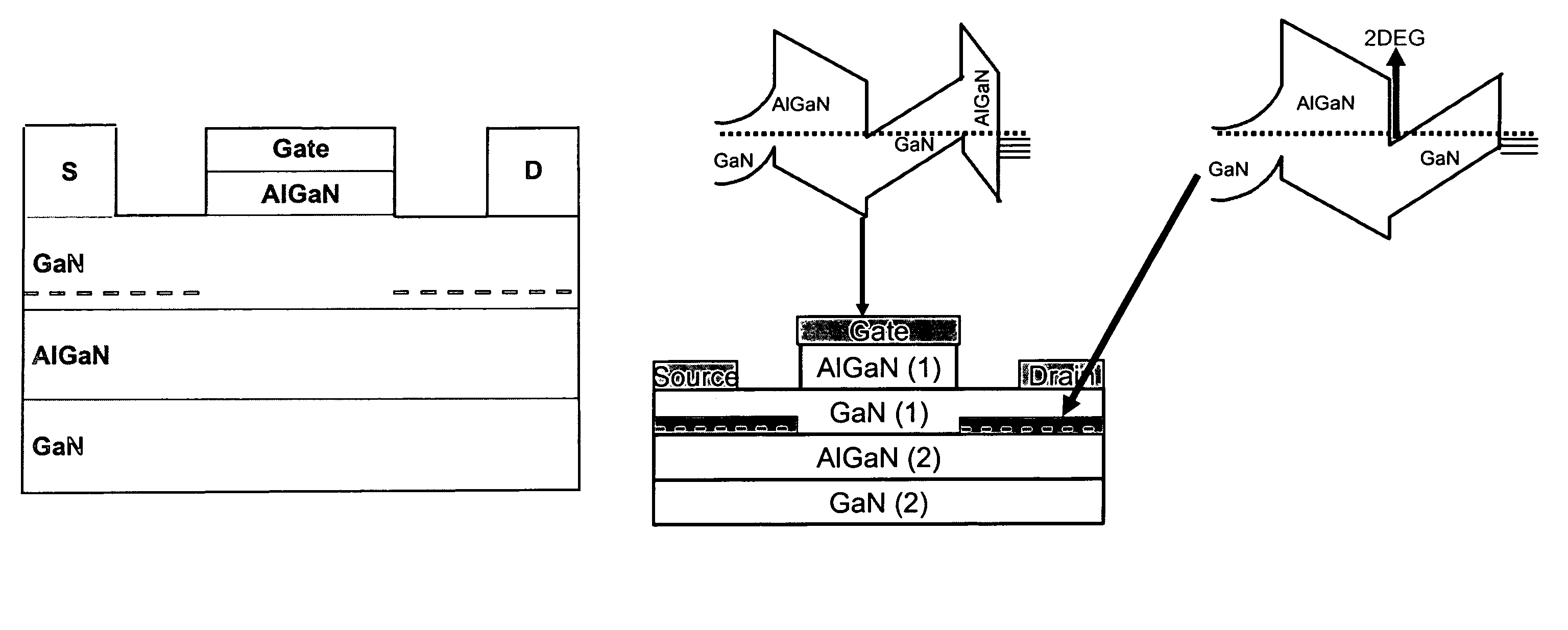
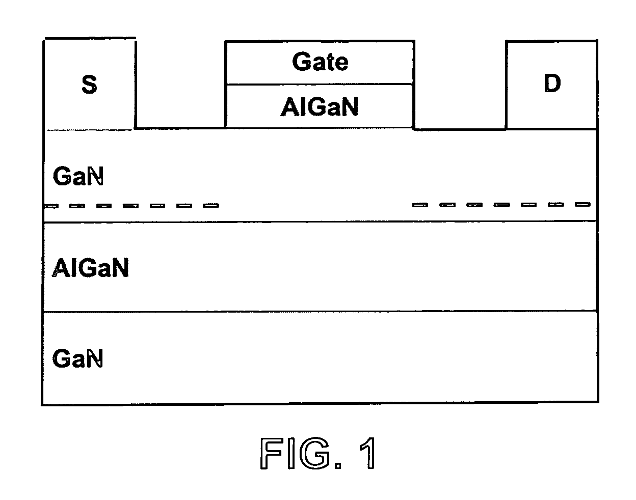
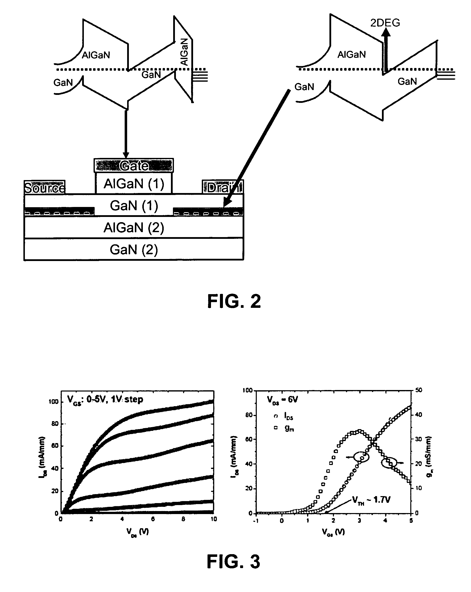
[0031]FIG. 1 is a cross-sectional schematic that discloses a novel enhancement mode HEMT transistor structure with a N-polar surface according to the preferred embodiment of the present invention. This transistor includes a gate, source (S) and drain (D), where the transistor has an epilayer structure under the gate as follows: AlGaN(1) / GaN(1) / AlGaN(2) / GaN(2) (numbered from top to bottom layers). The AlGaN(1) layer is grown thick enough so that polarization fields in this layer deplete the 2DEG at the AlGaN(2) / GaN(1) interface under zero gate bias. Under the access and contact...


PUM


Abstract

A novel enhancement mode field effect transistor (FET), such as a High Electron Mobility Transistors (HEMT), has an N-polar surface uses polarization fields to reduce the electron population under the gate in the N-polar orientation, has improved dispersion suppression, and low gate leakage.

Description

CROSS-REFERENCE TO RELATED APPLICATION[0001]This application claims the benefit under 35 U.S.C. Section 119(e) of the following co-pending and commonly-assigned U.S. patent application:[0002]U.S. Provisional Application Ser. No. 60 / 717,996, filed on Sep. 16, 2005, by Siddharth Rajan, Chang Soo Suh, James S. Speck, and Umesh K. Mishra, entitled “N-POLAR ALUMINUM GALLIUM NITRIDE / GALLIUM NITRIDE ENHANCEMENT-MODE FIELD EFFECT TRANSISTOR,”;[0003]which application is incorporated by reference herein.STATEMENT REGARDING FEDERALLY SPONSORED RESEARCH AND DEVELOPMENT[0004]This invention was made with Government support under Grant No. F49620-03-1-0235 awarded by AFOSR, and Grant No. H94003-04-2-0403 awarded by DARPA CNID. The Government has certain rights in this invention.BACKGROUND OF THE INVENTION[0005]1. Field of the Invention[0006]The invention is related to N-polar aluminum gallium nitride (AlGaN) / gallium nitride (GaN) enhancement mode field effect transistors (FETs), such as High Elect...

Claims


Application Information

Patent Timeline
Patent Type & Authority Patents(United States)
IPC IPC(8): H01L29/66
CPCH01L29/045H01L29/7784H01L29/7781H01L29/7783H01L29/432H01L29/2003
Inventor RAJAN, SIDDHARTHSUH, CHANG SOOSPECK, JAMES S.MISHRA, UMESH K.
Owner RGT UNIV OF CALIFORNIA
Why Eureka
Try Eureka