Method of manufacturing III nitride crystal, III nitride crystal substrate, and semiconductor device

a technology of nitride crystals and substrates, which is applied in the direction of crystal growth process, polycrystalline material growth, chemically reactive gases, etc., can solve the problems of reducing the yield of gan crystals

Active Publication Date: 2011-06-21
SUMITOMO ELECTRIC IND LTD
View PDF11 Cites 11 Cited by
  • Summary
  • Abstract
  • Description
  • Claims
  • Application Information

AI Technical Summary

Benefits of technology

[0015]An object of the present invention, to resolve the problems discussed above, is to make available a method of manufacturing III-nitride crystals, III-nitride crystal substrates, and semiconductor devices incorporating the III nitride crystal substrates, having a major surface whose variance in crystallographic plane orientation with respect to an {hkil} plane, being a crystallographic plane chosen exclusive of the {0001} form, is slight.

Problems solved by technology

With the method in the just-noted Patent Document 1, however, inasmuch as growth of the GaN crystal is carried out with, as seeds, the boules of crystal GaN that have been embedded into the sapphire substrate, due to the disparity in thermal expansion coefficient between sapphire and GaN, fractures and strain occur in the GaN crystal when the crystal is cooled following the growth process, such that GaN crystal of superior crystallinity has not been obtainable.
Furthermore, if III-nitride crystal containing Al—for example, AlxGayIn1−x−yN (x>0, y≧0, x+y≦1)—is grown by the method in above-noted Patent Document 1, because the Al precursor is not selective with respect to the silicon oxide film, the AlxGayIn1−x−yN grows onto the silicon oxide film as well, and consequently AlxGayIn1−x−yN crystal of superior crystallinity has not been obtainable.
Such inconsistency compromises the device properties of semiconductor devices that incorporate such nitride semiconductor layers, and is deleterious to production yields.

Method used


Image

  • Method of manufacturing III nitride crystal, III nitride crystal substrate, and semiconductor device
  • Method of manufacturing III nitride crystal, III nitride crystal substrate, and semiconductor device
  • Method of manufacturing III nitride crystal, III nitride crystal substrate, and semiconductor device

Examples


embodiments

1. Preparation of First GaN Crystal (First III-Nitride Crystal)

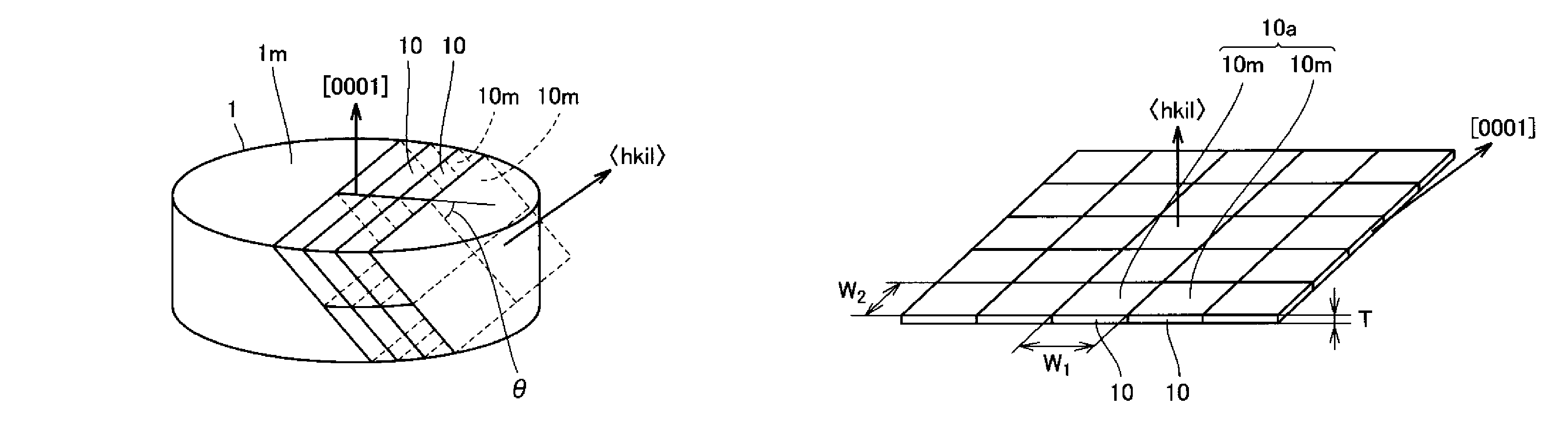
[0055]A 2-inch (50.8 mm) diameter GaN undersubstrate with a (0001)-plane major surface and a 2-mm radius of curvature (GaN undersubstrate A), and a 2-inch (50.8 mm) diameter GaN undersubstrate with a (0001)-plane major surface and a 5-mm radius of curvature (GaN undersubstrate B), obtained by slicing a GaN crystal grown by HVPE onto a 2-inch (50.8 mm) diameter sapphire substrate, were prepared.

[0056]First GaN crystal (first III-nitride crystal 1), of 12 mm thickness, was grown by HVPE onto the respective major surfaces of the thus-prepared GaN undersubstrate A and GaN undersubstrate B (cf. FIG. 1A). Here the first GaN crystal grown onto GaN undersubstrate A is termed “GaN crystal 1A,” while the first GaN crystal grown onto GaN undersubstrate B is termed “GaN crystal 1B.”

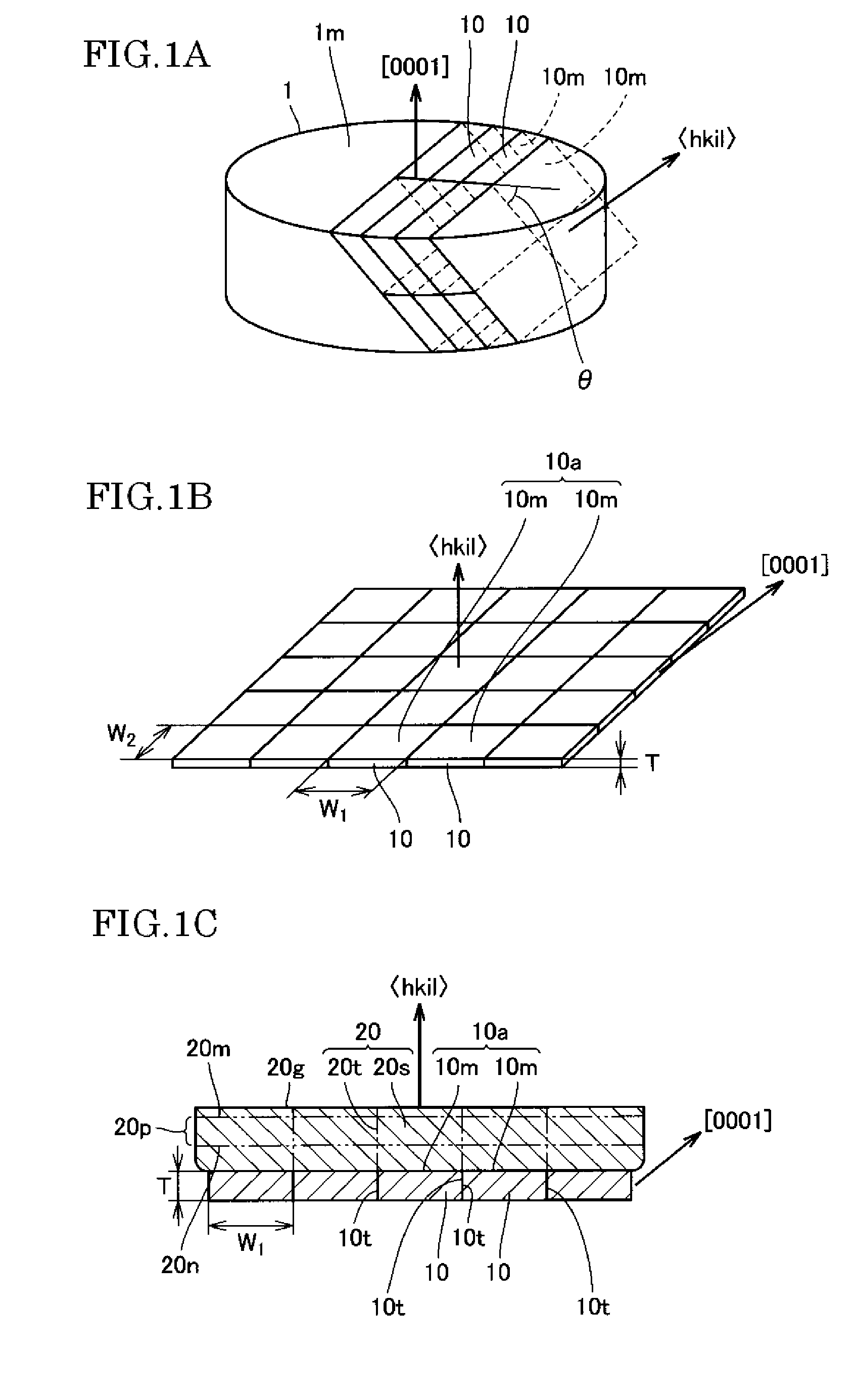
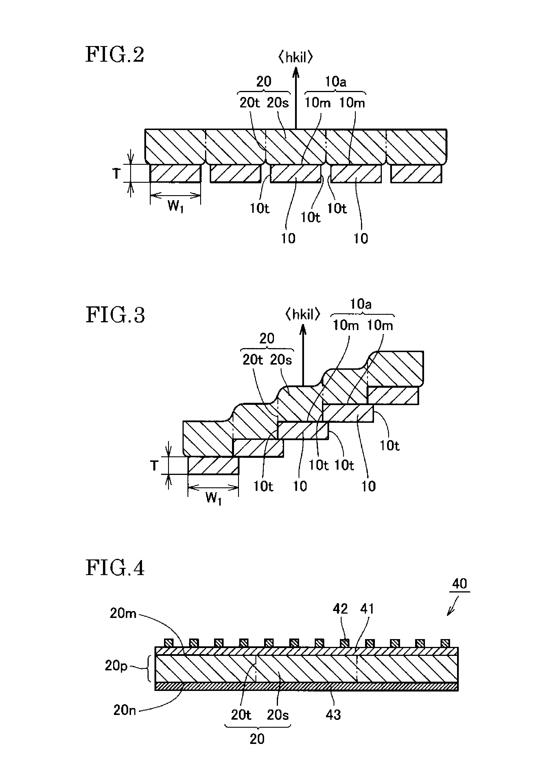
2. Conditioning of Crystal Plates

[0057]Referring to FIG. 1A, the GaN crystal 1A (first III-nitride crystal 1) was sliced along a plurality of planes havi...


PUM

PropertyMeasurementUnit
angleaaaaaaaaaa
angleaaaaaaaaaa
W2×thicknessaaaaaaaaaa

Abstract

Affords III-nitride crystals having a major surface whose variance in crystallographic plane orientation with respect to an {hkil} plane chosen exclusive of the {0001} form is minimal. A method of manufacturing the III-nitride crystal is one of: conditioning a plurality of crystal plates (10) in which the deviation in crystallographic plane orientation in any given point on the major face (10m) of the crystal plates (10), with respect to an {hkil} plane chosen exclusive of the {0001} form, is not greater than 0.5°; arranging the plurality of crystal plates (10) in a manner such that the plane-orientation deviation, with respect to the {hkil} plane, in any given point on the major-face (10m) collective surface (10a) of the plurality of crystal plates (10) will be not greater than 0.5°, and such that at least a portion of the major face (10m) of the crystal plates (10) is exposed; and growing second III-nitride crystal (20) onto the exposed areas of the major faces (10m) of the plurality of crystal plates (10).

Description

BACKGROUND OF THE INVENTION[0001]1. Technical Field[0002]The present invention relates to methods of manufacturing III-nitride crystals and III-nitride crystal substrates having a major surface whose variance in crystallographic plane orientation, with respect to an {hkil} plane that is a crystallographic plane chosen exclusive of the {0001} form, is slight (h, k, i and l herein being whole numbers, with the relationship i=−(h+k) holding—likewise hereinafter). The present invention also relates to methods of manufacturing semiconductor devices including such III nitride crystal substrates.[0003]2. Description of the Related Art[0004]Group-III nitride crystals, which are employed advantageously in light-emitting devices, electronic devices and semiconductor sensors, are ordinarily manufactured by growing crystal onto the major surface of a sapphire substrate having a (0001)-plane major surface, or onto a GaAs substrate having a (111) a-plane major surface, by means of a vapor-phase t...

Claims


Application Information

Patent Timeline
Patent Type & Authority Patents(United States)
IPC IPC(8): H01L21/205H01L21/208C30B9/00C30B25/18C30B29/38
CPCC30B9/04C30B19/02C30B29/403C30B25/20C30B19/12
Inventor FUJIWARA, SHINSUKE
Owner SUMITOMO ELECTRIC IND LTD
Why Eureka
Try Eureka