However, by using the die-to-
database comparison method for
wafer inspection, corner roundness of a pattern formed on a wafer is likely to be detected as a defect.
However, in the inspection of a wafer, because the corner roundness added by the pretreatment may be different from corner roundness of each pattern actually formed on the wafer, the pretreatment may not perfectly prevent the corner roundness of the pattern from being detected as the defect.
As a result, a problem in which a fine defect existing in a place except a corner cannot be detected has happened.
However, the above problem is severe for the die-to-
database comparison wafer inspection, because a pattern formed on the wafer is allowed to be deformed as long as an electrical property is guaranteed.
Therefore, the die-to-
database comparison wafer inspection has not been put into practical use.
Because the repeated defects occur in a die to-be-inspected and in adjacent dies that are to be compared with the die to-be-inspected, the die-to-die comparison wafer inspection cannot detect the repeated defects.
Although the die-to-die comparison wafer inspection has not been put into practical use because of calculation cost or the like, there have been proposed inspection methods in which
design data and a wafer image are used.
However, these methods fail to realize an inspection speed that is
usable in high-speed inspection, and fail to perform matching while detecting a pattern deformation quantity.
However, the method cannot classify whether the defect is a killer defect or not, because the method cannot recognize which part of a circuit the defect destroys.
Moreover, a position of a defect detected by the die-to-die comparison inspection has an error caused by precision of a stage and an
image generation device of an inspection apparatus, and such error is approximately ten or more times larger than a
line width of a pattern to-be-inspected.
Due to the error, even if a defect position is related with design data, relationship between the defect position and the design data cannot be recognized.
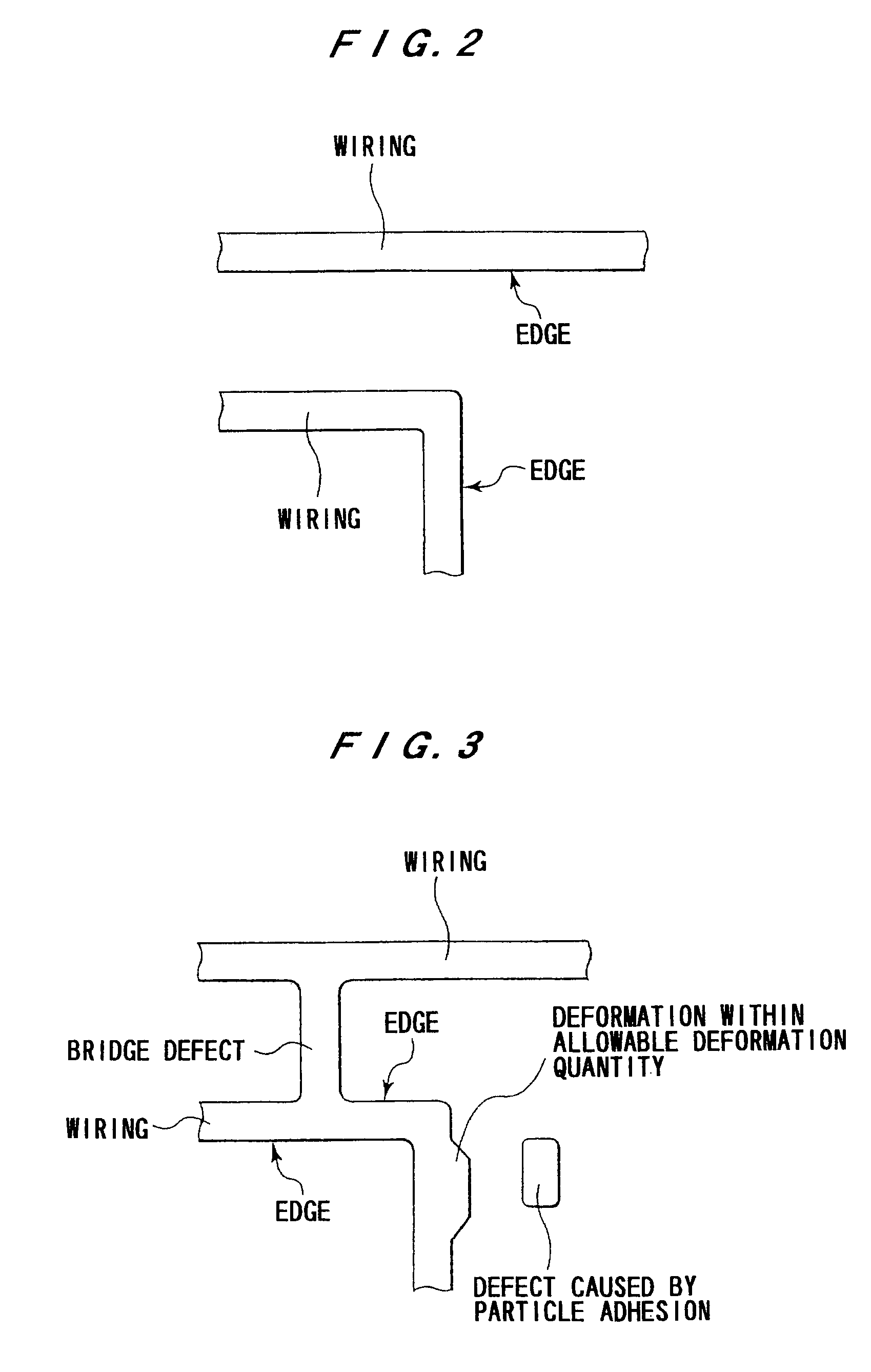
If the OPC pattern does not effectively correct a pattern formed on a wafer, repeated defects occur.
However, the die-to-die comparison wafer inspection cannot detect the repeated defects.
In addition, in a multi-product / small-volume fabricating process, e.g. a
system-on-a-
chip (SoC) fabricating process, a short delivery time is required.
In the fabricating process, when repeated defects are detected in electric inspection as a final inspection, a short delivery time cannot be achieved.
Although the entire device can be verified by the
lithography simulator, the
simulation pattern cannot be necessarily the same as an actual pattern.
Moreover, a defect except for a defect caused by the OPC pattern cannot be detected by the
lithography simulator.
However, currently, the control of the two-dimensional shape is performed by a human work, and is not perfectly performed.
1. The method, in which the inspection is performed for every profile acquisition section, is used. However, by using such local
inspection method, deformation for every pattern to-be-inspected cannot be inspected.
2. It is necessary to detect bridge state of a pattern to-be-inspected, which is a
negative pattern in a wiring layer, in higher speed. Further, it is necessary to reduce an effect of an
electron beam spot size.
3. In the case where a pattern to-be-inspected, which is a
negative pattern in a wiring layer and has a larger
line width than an
electron beam spot size, does not exist, it is necessary to prevent deterioration of defect detection accuracy of a pattern to-be-inspected, which is a
negative pattern in a wiring layer and has the smaller
line width than the
electron beam spot size.
4. Conventionally, an
overlay error caused in process of the double
exposure method is controlled by measuring limited areas in a
semiconductor device. Therefore, the
overlay error caused locally by a
stepper aberration or the like cannot be controlled.
5. In the case of long-term inspection, it may be necessary to adjust a setting value of an
image generation device. In such case, it is necessary that the most suitable setting value of the image generation device is estimated and the setting value of the image generation device is adjusted by using the estimated setting value.
6. A method of controlling OPC patterns of gates by using a line width and space widths on both sides of gates has been used. Because space widths on both sides of a gate having different space widths on one side cannot be determined uniquely, OPC patterns of the gate cannot be controlled.
7. A part of a pattern to-be-inspected fabricated by a
stepper under a focus condition and an
exposure dose condition, which are different from the optimal conditions, may be deformed more than an allowable deformation quantity. In such case, pattern deformation quantities cannot be obtained from the above-mentioned part.

