Method for direct fabrication of nanostructures

a nanostructure and fabrication method technology, applied in the field of microfabrication, can solve the problems of easy damage to nanoscale devices such as dna and proteins, difficult to produce sub-100 nm structures, and organic materials

Active Publication Date: 2011-08-16
MASSACHUSETTS INST OF TECH
View PDF12 Cites 5 Cited by
  • Summary
  • Abstract
  • Description
  • Claims
  • Application Information

AI Technical Summary

Benefits of technology

[0011]It is an object of the present invention to achieve direct deposition ...

Problems solved by technology

Known microfabrication techniques such as photolithography, microcontact printing, micromachining, and microwriting can produce patterns as small as 100 nm, but the production of sub-100 nm structures still poses a challenge.
Furthermore, many organic materials that could be useful in nanoscale devices, such as DNA and proteins, are easily damaged and, thus, are difficult to pattern to form very small structures.
However, the pushing operations are very complex, and construction of useful structures is indirect and often prohibitively tedious.
Problems that arise with DPN technology stem from the dependence of this technique on the liquid meniscus and chemical affinity of the patterning material to the substrate.
Solubility characteristics o...

Method used


Image

  • Method for direct fabrication of nanostructures
  • Method for direct fabrication of nanostructures
  • Method for direct fabrication of nanostructures

Examples


Embodiment Construction

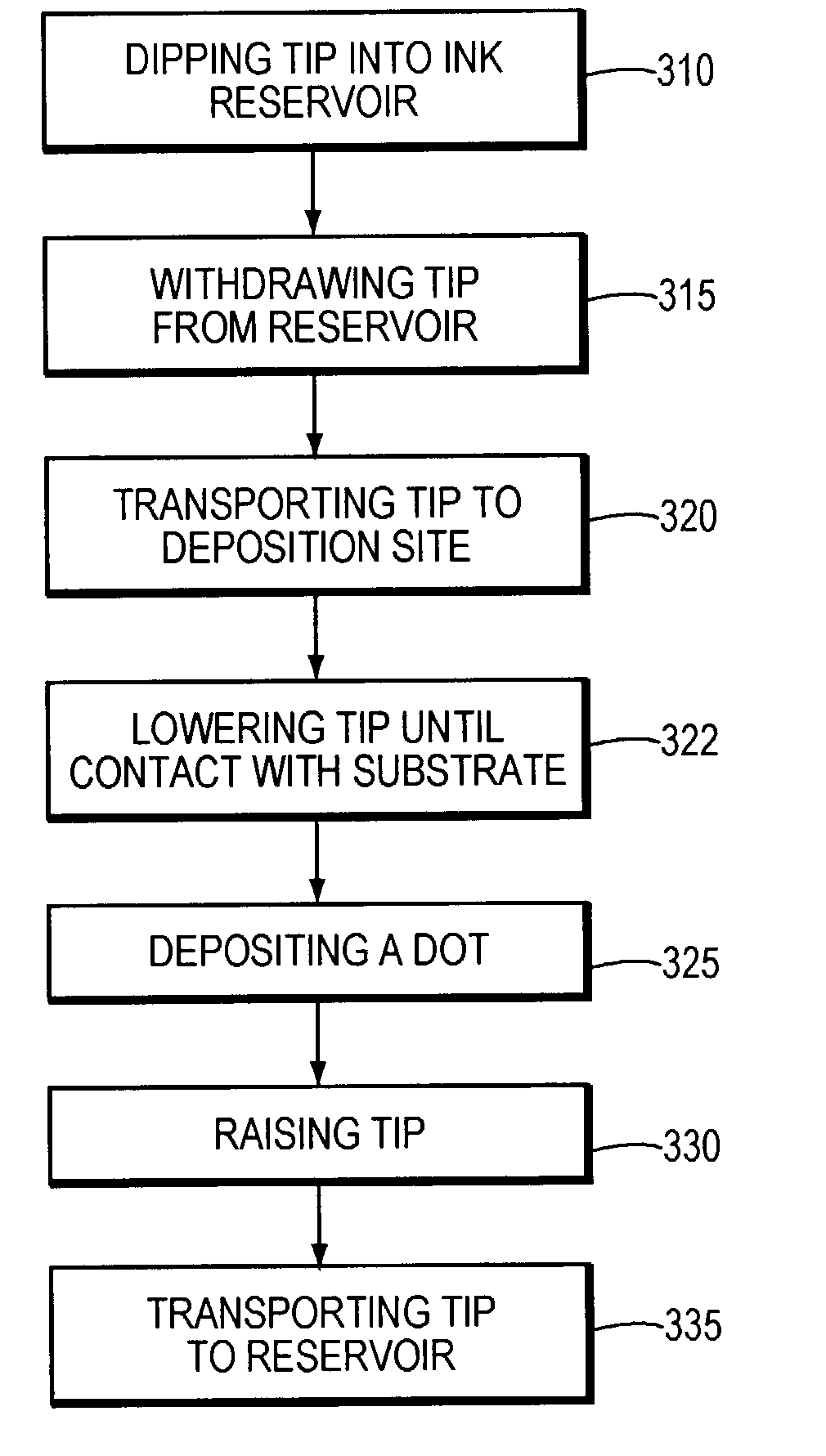
[0051]The nanoassembly method of the invention provides for the deposition of planar, multi-layer, and three-dimensional nanostructures. In particular, the nanoassembly system can be used for the fabrication of a number of basic canonical structures including lines, dots, and columns. These canonical structures can be combined and adjacently deposited laterally and / or vertically to form complicated and useful structures, devices, and patterns.

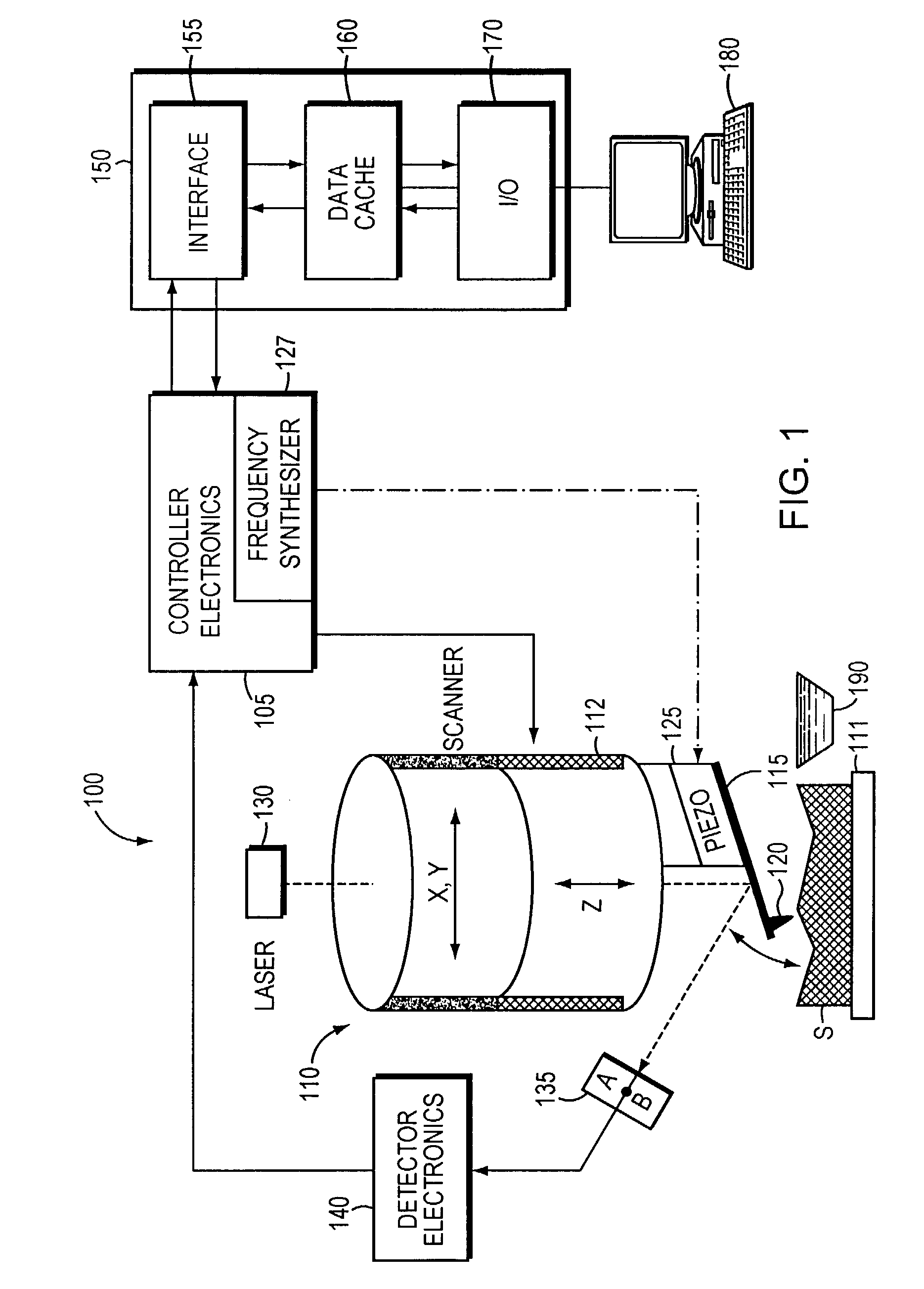
[0052]Referring to FIG. 1, in one embodiment, a nanoassembly apparatus 100 in accordance with the invention includes a controller 105 that operates an AFM head 110 in three dimensions over the surface of a substrate S disposed on top of an adjustable substrate positioning stage 111. As illustrated in FIG. 1, the surface of substrate S extends in the (x,y) plane, while movement toward and away from the surface occurs along the z axis. A transport mechanism may execute movement along the three axes using a series of independently operable piezo e...


PUM

PropertyMeasurementUnit
Widthaaaaaaaaaa
Widthaaaaaaaaaa
Forceaaaaaaaaaa

Abstract

An all-additive method for direct fabrication of nanometer-scale planar and multilayer structures comprises the steps of acquiring a transferable material with a submillimeter-scale tip, depositing at least a portion of the acquired first transferable material at a predetermined location onto a substrate without a bridging medium, and repeating to create a structure using the transferable material.

Description

RELATED APPLICATION[0001]This application claims priority to and the benefits of U.S. Ser. No. 60 / 357,006, filed on Feb. 14, 2002, the entire disclosure of which is hereby incorporated by reference.FIELD OF THE INVENTION[0002]The present invention generally relates to the field of microfabrication, in particular, to direct fabrication and imaging of nanometer-scale structures using a scanning probe microscope, e.g. an atomic force microscope.BACKGROUND OF THE INVENTION[0003]Nanotechnologies promise to bring about the advent of very small, yet important electronic and biological devices with features that are only a few tens of nanometers across. A variety of nanometer-scale (“nano”) materials, such as carbon nanotubes, nanoparticles, and molecular memories are being developed. However, improvements in the handling and patterning of these nanomaterials are necessary before they can be cost-effectively incorporated into useful nanodevices such as, for example, single-electron transist...

Claims


Application Information

Patent Timeline
IPC IPC(8): B05D5/00B05D7/00B05D1/34B05D1/36B82B3/00G01Q60/00G01Q70/08G03F7/00
CPCB82B3/00B82Y10/00B82Y30/00B82Y40/00G03F7/0002Y10S977/855Y10S977/851Y10S977/86Y10S977/849Y10S977/85
Inventor HUBERT, BRIANJACOBSON, JOSEPHBLETSAS, AGGELOS
Owner MASSACHUSETTS INST OF TECH
Why Eureka
Try Eureka