Dynamic push for topological routing of semiconductor packages
a topological routing and semiconductor technology, applied in the field of electronic design automation, can solve the problems of limited locations, inflexible 1.5 d routing, and difficult off-chip routing, and achieve the effect of reducing the length of the first wir
- Summary
- Abstract
- Description
- Claims
- Application Information
AI Technical Summary
Benefits of technology
Problems solved by technology
Method used
Image
Examples
Embodiment Construction
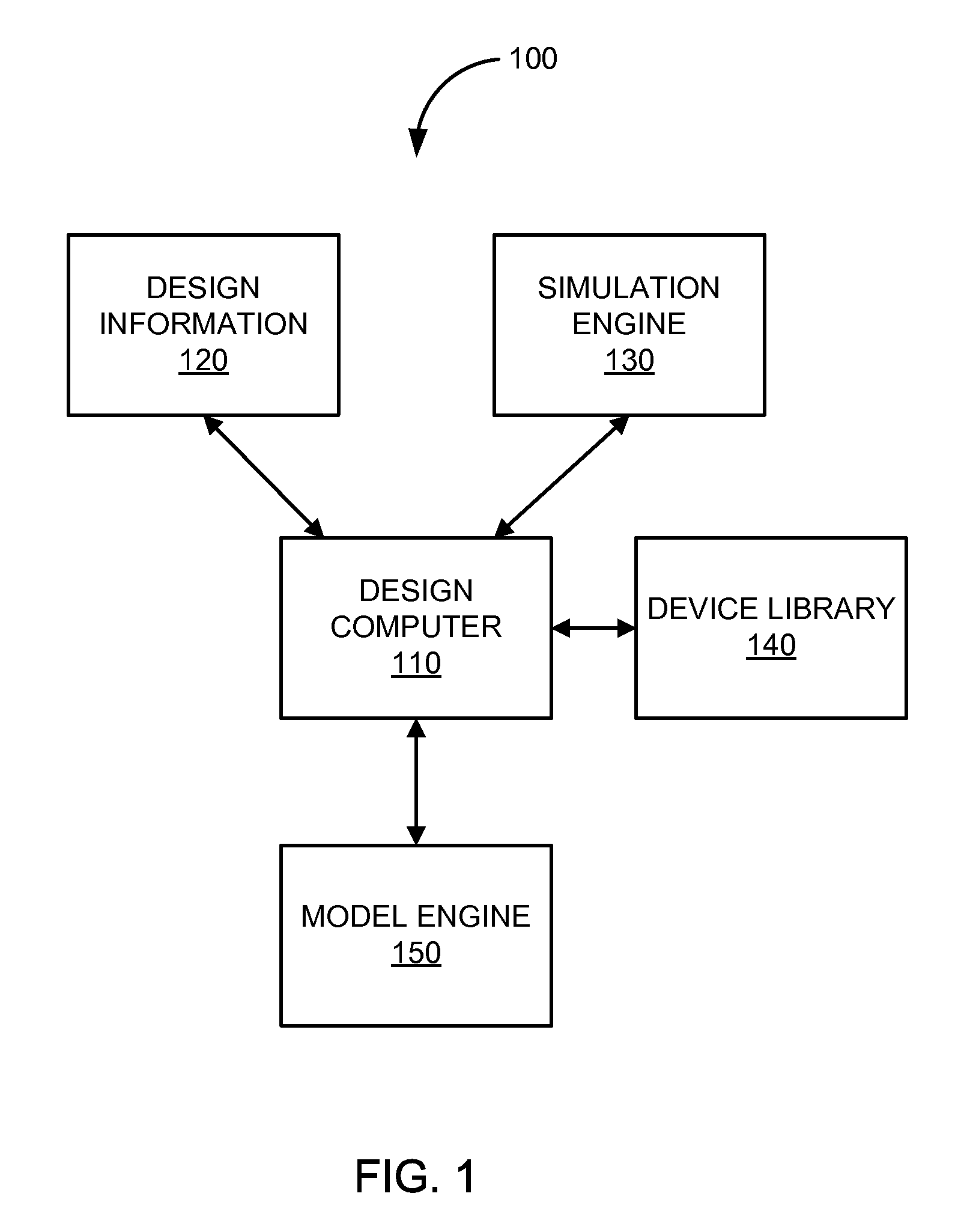
[0048]FIG. 1 is a simplified block diagram of electronic design automation (EDA) system 100 that may be used for topological routing of semiconductor packages in one embodiment of the present invention. System 100 can include design computer 110 coupled to design information 120, simulation engine 130, device library 140, and model engine 150.
[0049]In various embodiments, a user may interact with or otherwise use design computer 110 to design and produce electronic systems ranging from printed circuit boards (PCBs) to integrated circuits. The user may use design computer 110 (along with design information 120, simulation engine 130, device library 140, and model engine 150) of system 100 to perform co-design and architecture of packages and integrated circuits.
[0050]In some embodiments, the user may interact with or otherwise use design computer 110 to perform design tasks, such as floorplanning, placement, routing, or other steps for creating an integrated circuit. In one embodimen...
PUM
 Abstract
Description
Claims
Application Information


