Method for manufacturing semiconductor device including hat-shaped gate electrode

a technology of semiconductor devices and gate electrodes, which is applied in the direction of semiconductor devices, basic electric elements, electrical appliances, etc., can solve the problems of not working effectively in suppressing off current, not working effectively in preventing deterioration, and not being able to achieve the effect of reducing manufacturing costs, improving yield and preferable operating characteristics

Inactive Publication Date: 2011-08-30
SEMICON ENERGY LAB CO LTD
View PDF92 Cites 6 Cited by
  • Summary
  • Abstract
  • Description
  • Claims
  • Application Information

AI Technical Summary

Benefits of technology

[0031]According to the present invention, a fine hat-shaped gate electrode can be formed, and an LDD region having an LDD length that cannot be accomplished conventionally can be formed by doping an impurity element with the use of this gate electrode as a mask. Therefore, in spite of miniaturization, a high-reliability semiconductor device with preferable operating characteristics can be realized; thus, semiconductor devices appropriate for various circuits can be manufactured separately. Moreover, semiconductor devices can be manufactured separately in a process having a few processing step; therefore, the manufacturing cost can be reduced and the yield can be improved.
[0032]Further, a submicron TFT in a desired size can be formed without limiting the size, and a semiconductor device itself can be extremely compact and lightweight. Moreover, an LDD length appropriate for each TFT can be designed; thus, a semiconductor device in which desired ON current can be ensured as well as suppressing short-channel effect and increasing withstand pressure can be obtained.
[0033]Furthermore, sidewalls are formed on the sides of a hat-shaped gate electrode and an impurity element is doped; therefore, a high-reliability semiconductor device capable of suppressing short channel effect and having both a Loff region and a Lov region can be realized.

Problems solved by technology

A conventional thin film transistor (Thin Film Transistor: hereinafter, referred to as TFT) is formed of an amorphous semiconductor film; therefore, it is almost impossible to obtain a TFT having field effect mobility of 10 cm2 / V·Sec or more.
Here, the Loff region works effectively in suppressing OFF current, whereas it does not work effectively in preventing the deterioration in ON current due to hot carriers by alleviating the electric field in the vicinity of the drain.
On the other hand, the Lov region works effectively in preventing the decrease in ON current by relieving the electric field in the vicinity of the drain; however, it does not work effectively in suppressing OFF current.
However, it is difficult to form a minute TFT appropriate for various circuits by using the method described in Reference 1.
However, it is difficult to adjust the taper angle and, on the other hand, when θ is 90°, the LDD region itself cannot be formed; therefore, it is difficult to form an LDD length of a certain value or less.
However, in the conventional method, although the length of a gate electrode and a semiconductor film can be formed in a submicron size by etching, it is difficult to provided an LDD region having an LDD length in accordance with its size.
Thus, it is difficult to obtain a submicron TFT having a preferable characteristic.
Furthermore, in terms of a manufacturing cost, it is required to develop a method for manufacturing a semiconductor device in which TFTs appropriate for each circuit are manufactured simultaneously in a process with a few processing step.

Method used


Image

  • Method for manufacturing semiconductor device including hat-shaped gate electrode
  • Method for manufacturing semiconductor device including hat-shaped gate electrode
  • Method for manufacturing semiconductor device including hat-shaped gate electrode

Examples


embodiment mode 1

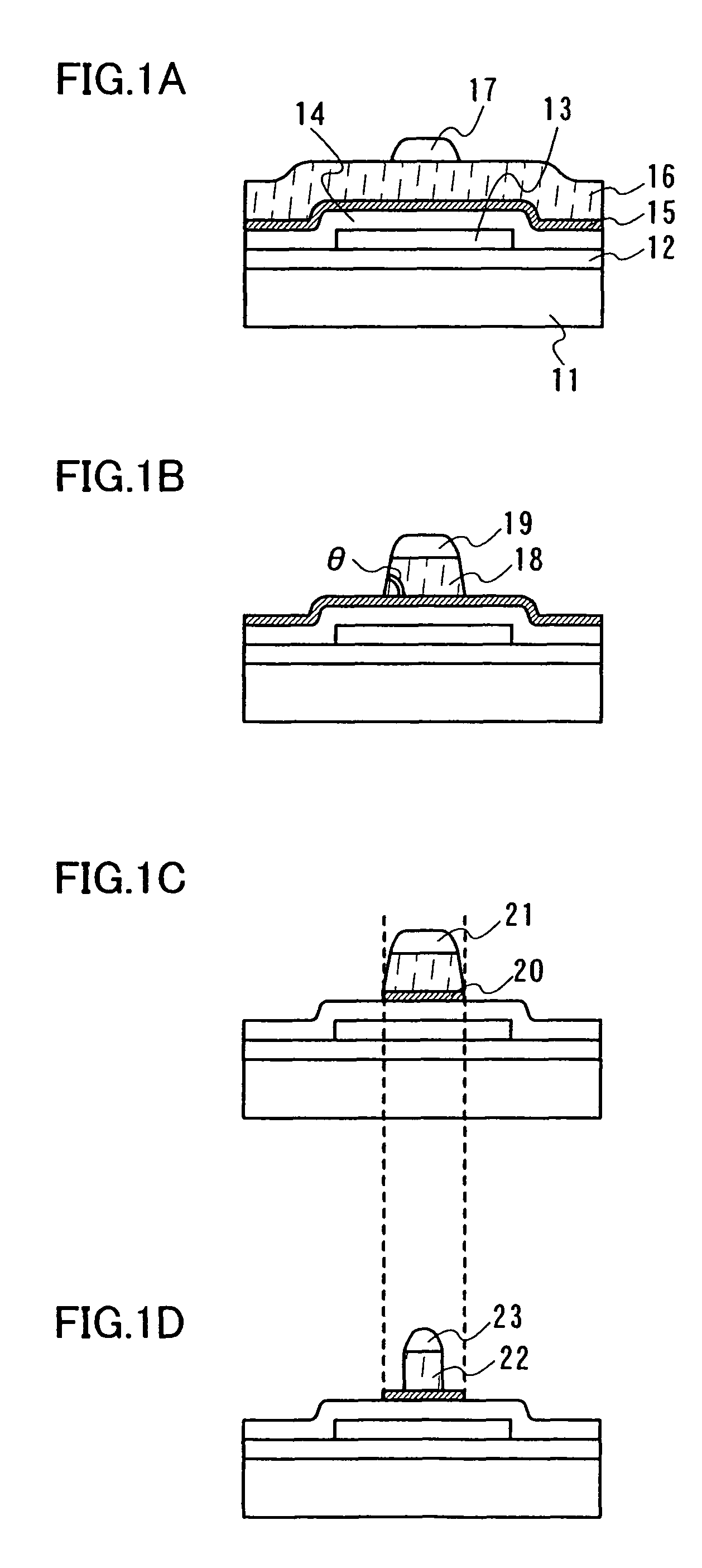
[0068]Hereinafter, a method for manufacturing a semiconductor device according to Embodiment Mode 1 is shown with reference to FIGS. 1A to 1D and FIGS. 2A to 2C. A TFT used in the semiconductor device of this embodiment mode has an LDD region of a Lov region or a Loff region.

[0069]First, a base insulating film 12 is formed over a substrate 11 in a thickness of 100 nm to 300 nm. The substrate 11 may be an insulating substrate such as a glass substrate, a quartz substrate, a plastic substrate, or a ceramic substrate; a metal substrate; a semiconductor substrate; or the like.

[0070]The base insulating film 12 can be formed using a single layer structure or a multilayer structure of an insulating film having oxygen or nitrogen such as silicon oxide (SiOx), silicone nitride (SiNx), silicon oxynitride (SiOxNy) (x>y), or silicon nitride oxide (SiNxOy) (x>y). It is preferable to form a base insulating film in particular when impurities from a substrate are concerned.

[0071]In addition, it pre...

embodiment mode 2

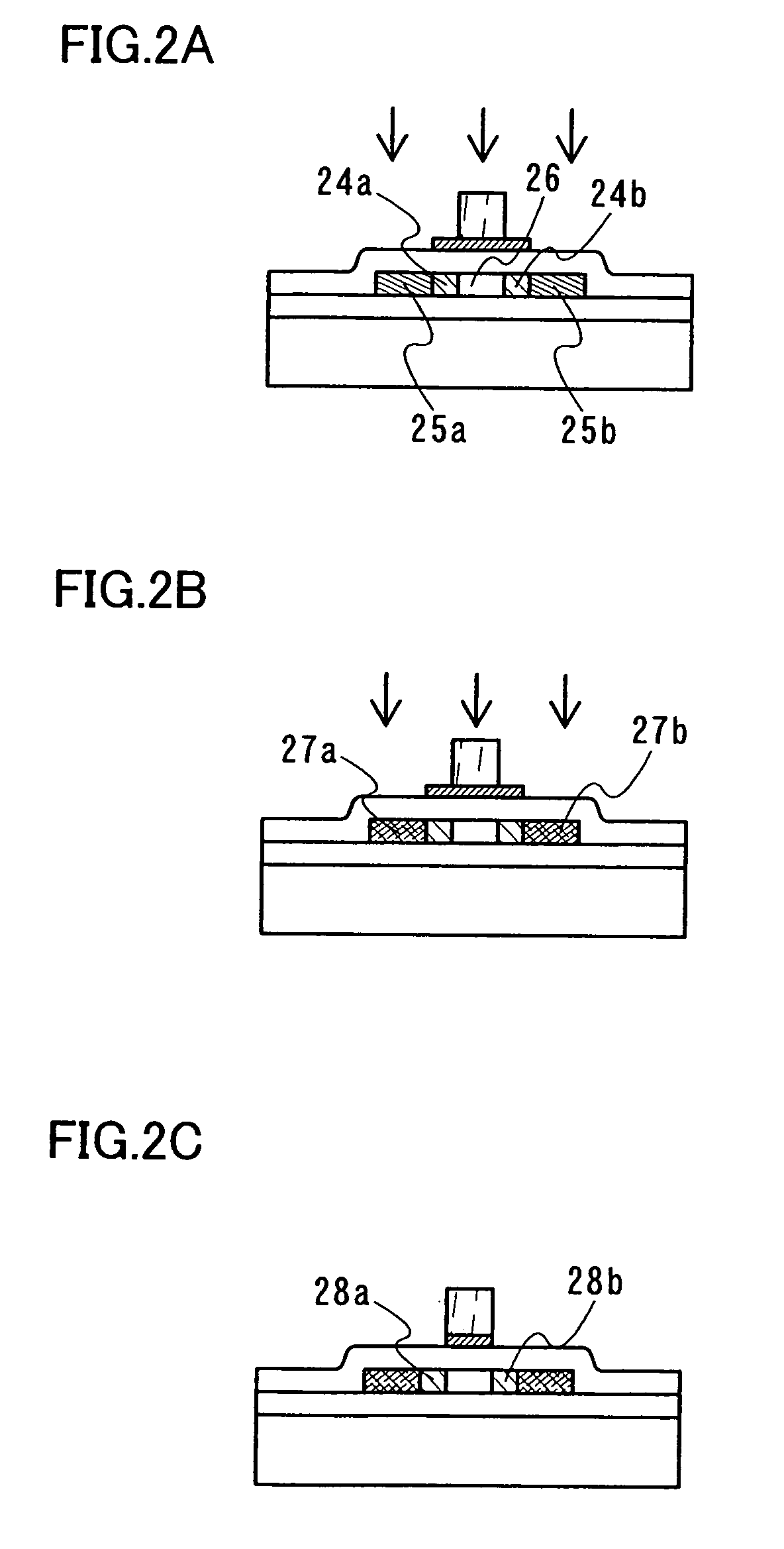
[0102]This embodiment mode shows a method for manufacturing a semiconductor device having a Loff region with reference to FIGS. 3A to 3C.

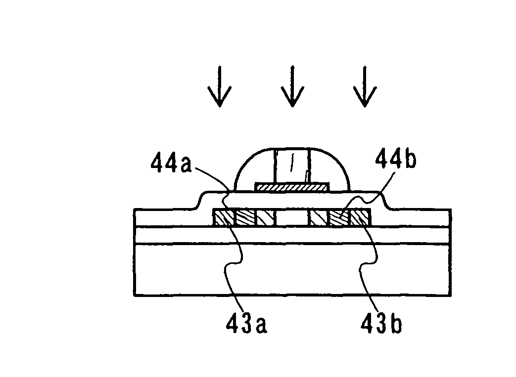
[0103]In this embodiment mode, a TFT having a hat-shaped gate electrode is formed in the same steps as Embodiment Mode 1 in FIGS. 1A to 1D to obtain a state shown in FIG. 3A.

[0104]Thereafter, the island-shaped semiconductor film not overlapped with the second gate electrode 20 is partially doped with an impurity element by performing a first doping using the second and the third gate electrodes as masks (FIG. 3B). Through this doping, low-concentration impurity regions 31a and 31b and a channel-forming region 35 are formed. The doping is performed so that the concentrations of the impurity elements in the low-concentration impurity regions 31a and 31b are each 1×10¹⁶ atoms / cm3 to 1×10²⁰ atoms / cm3, preferably 1×10¹⁶ atoms / cm3 to 5×10¹⁸ atoms / cm3.

[0105]Next, a second doping for forming high-concentration impurity regions is performed (FIG. 3C). A res...

embodiment mode 3

[0108]This embodiment mode explains a method for manufacturing a semiconductor device having-both a Lov region and a Loff region with reference to FIGS. 4A to 4D. In this embodiment mode, a TFT having a hat-shaped gate electrode and an impurity region is formed in the same steps as Embodiment Mode 1 in FIGS. 1A to 2A (FIG. 4A).

[0109]Next, a film 41 formed from a silicon compound is formed over the gate electrode in 100 nm thick by using a known film forming method (FIG. 4B). In this embodiment mode, a silicon oxide film is used as the film 41. Then, sidewalls 42 shown in FIG. 4C are formed by etching back the film 41 formed from a silicon compound. When the difference between the gate length of the second gate electrode and that of the third gate electrode is extremely small, the sidewalls 42 are formed so that not only the side surfaces of the third gate electrode but also those of the second gate electrode are covered.

[0110]Then, a second doping is performed as shown in FIG. 4D. T...


PUM


Abstract

It is an object of the present invention to manufacture a TFT having a small-sized LDD region in a process with a few processing step and to manufacture TFTs each having a structure depending on each circuit separately. According to the present invention, a gate electrode is a multilayer, and a hat-shaped gate electrode is formed by having the longer gate length of a lower-layer gate electrode than that of an upper-layer gate electrode. At this time, only the upper-layer gate electrode is etched by using a resist recess width to form the hat-shaped gate electrode. Accordingly, an LDD region can be formed also in a fine TFT; thus, TFTs having a structure depending on each circuit can be manufactured separately.

Description

FIELD OF THE INVENTION[0001]The present invention relates to a semiconductor device formed of various circuits and a manufacturing method thereof.DESCRIPTION OF THE RELATED ART[0002]A conventional thin film transistor (Thin Film Transistor: hereinafter, referred to as TFT) is formed of an amorphous semiconductor film; therefore, it is almost impossible to obtain a TFT having field effect mobility of 10 cm2 / V·Sec or more. However, a TFT having high filed effect mobility can be obtained owing to the appearance of a TFT formed of a crystalline semiconductor film.[0003]Since the TFT formed of crystalline semiconductor films has high field effect mobility, various functional circuits can be formed over one substrate simultaneously by using the TFT. For example, in a display device, previously, a driver IC and the like are mounted on a display portion to have a driver circuit. On the other hand, the use of the TFTs formed of crystalline semiconductor films enables a display portion and a ...

Claims


Application Information

Patent Timeline
Patent Type & Authority Patents(United States)
IPC IPC(8): H01L21/00
CPCH01L27/1214H01L27/1266H01L29/78621H01L29/66757H01L2029/7863H01L27/127H01L29/42384
Inventor YAMAGUCHI, MAYUMIISOBE, ATSUOSAITO, SATORU
Owner SEMICON ENERGY LAB CO LTD
Why Eureka
Try Eureka