Printed circuit board reinforcement structure and integrated circuit package using the same

a technology of integrated circuits and printed circuit boards, which is applied in the direction of dielectric characteristics, lighting and heating apparatus, and stress/warp reduction of printed circuits, etc., can solve the problems of reduced rigidity (mechanical deformation of printed circuit boards, and deterioration of reliability, so as to maintain the structural rigidity ( mechanical strength) of printed circuit boards. , to achieve the effect of not increasing the thickness of printed circuit boards

Inactive Publication Date: 2011-11-15
SAMSUNG ELECTRONICS CO LTD
View PDF12 Cites 52 Cited by
  • Summary
  • Abstract
  • Description
  • Claims
  • Application Information

AI Technical Summary

Benefits of technology

[0011]Accordingly, the present invention has been made to solve the above-mentioned problems occurring in the prior art, and the present invention provides a printed circuit board reinforcement structure which does not increase the thickness of a printed circuit board, and is capable of maintaining structural rigidity (mechanical strength) of the printed circuit board, without substantially changing the material and design of a printed circuit board, and to provide an integrated circuit package using such a printed circuit board reinforcement structure.
[0012]In addition, the present invention provides an integrated circuit package, wherein the method employs a printed circuit board having a thickness of not more than 1.0 mm, so that the thickness of the integrated circuit package can be reduced, and the strength of the printed circuit board can be increased.
[0013]According to an aspect of the present invention, there is provided a printed circuit board reinforcement structure for reinforcing the rigidity of a printed circuit board with a plurality of surface mounting devices, including a hard layer having one or more openings formed at areas corresponding to one or more surface mounting devices with a thickness exceeding a predetermined thickness, so that the openings can receive the corresponding surface mounting devices among the surface mounting devices mounted on the printed circuit board, respectively; and a soft layer bonded to a side of the hard layer so that the soft layer can accommodate the protrusion of the surface mounting devices.
[0021]According to another aspect of the present invention, there is a provided an integrated circuit package including a printed circuit board with a plurality of surface mounting devices; a hard layer having one or more openings formed at areas corresponding to one or more surface mounting devices with a thickness exceeding a predetermined thickness, so that the openings can receive the corresponding surface mounting devices among the surface mounting devices mounted on the printed circuit board, respectively; and a soft layer bonded to a side of the hard layer so that the soft layer can acconmmodate the protrusion of the surface mounting devices.

Problems solved by technology

In general, however, if the thickness of a printed circuit board is reduced, the rigidity (mechanical strength) of the printed circuit board is also reduced, whereby the printed circuit board is subjected to deformation, such as flexure, distortion, etc., and its reliability is deteriorated.
Therefore, the practical lower limit for printed circuit board thickness has been limited to about 1.0 mm up to now.
However, this conventional method induces a quality problem, such as the deterioration of molding workability, and a difficult recycling problem due to the use of a material harmful for human body and environment.
However, according to this method, the processes for making the mold come into close contact with the printed circuit board, and introducing the resin are very complicated.
In addition, since resin residue remains in a gap between the printed circuit board and the mold, a post process for smoothing the surfaces of the printed circuit board is required.
Consequently, this method is not suitable for mass production.
Specifically, there is a disadvantage in that the resin contracts while it is being cured, thereby rendering the printed circuit board warped.
However, the length of time required for spraying the resin is long.
Consequently, this method is also not suitable for mass production.

Method used


Image

  • Printed circuit board reinforcement structure and integrated circuit package using the same
  • Printed circuit board reinforcement structure and integrated circuit package using the same
  • Printed circuit board reinforcement structure and integrated circuit package using the same

Examples


Embodiment Construction

[0026]Hereinafter, exemplary embodiments of the present invention will be described with reference to the accompanying drawings. It should be noted that in the following description, the same elements will be designated by the same reference numerals even though they are shown in different drawings. In addition, in the following description of the present invention, a detailed description of known functions and configurations incorporated herein will be omitted for clarity and conciseness.

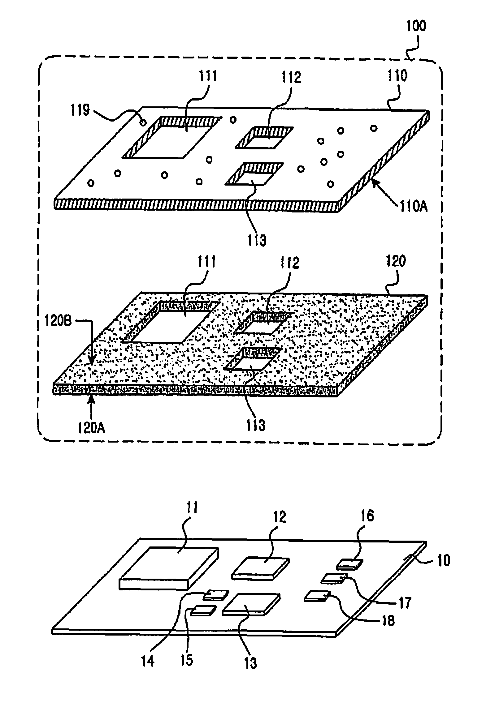
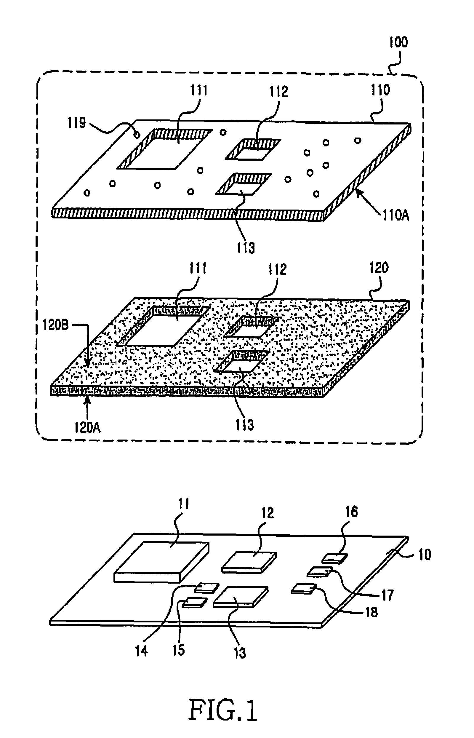
[0027]FIG. 1 is a schematic perspective view for illustrating a construction of a printed circuit board reinforcement structure according to an embodiment of the present invention. For the convenience of description, the printed circuit board reinforcement structure is depicted together with a printed circuit board 10, on which a plurality of SMDs (Surface Mounting Devices) is mounted.

[0028]Referring to FIG. 1, the printed circuit board reinforcement structure 100 includes a hard layer 110 and a so...


PUM


Abstract

A printed circuit board reinforcement structure for a printed circuit board receiving a plurality of surface mounting devices, and an integrated circuit package using the same. The structure includes a hard layer having one or more openings formed at areas corresponding to one or more surface mounting devices with a thickness exceeding a predetermined thickness; and a soft layer bonded to a side of the hard layer so that the soft layer can accommodate the protrusion of the surface mounting devices. The structure prevents defects of a printed circuit board, such as deformation, fracture or the like, while substantially reducing the size of a package by applying a reinforcement structure to a thin printed circuit board, thereby reinforcing the rigidity (mechanical strength) of the thin printed circuit board.

Description

PRIORITY[0001]This application claims the priority under 35 U.S.C. §119(a) to an application filed in the Korean Industrial Property Office on Jul. 31, 2007 and assigned Serial No. 2007-77047, the contents of which are hereby incorporated by reference.BACKGROUND OF THE INVENTION[0002]1. Field of the Invention[0003]The present invention relates to an IC (Integrated Circuit) package, and in particular to a PCB (Printed Circuit Board) reinforcement structure for preventing the deformation of and damage to a thin printed circuit board (for example, a printed circuit board having a thickness of not more than 0.4 mm), and an integrated circuit package using the same.[0004]2. Description of the Related Art[0005]Recently, due to the miniaturization, thinning, and weight reduction of electronic appliances, highly integrated circuit packages are required. For this reason, the super-thin design of printed circuit boards is also required.[0006]A printed circuit board serves to mechanically fix ...

Claims


Application Information

Patent Timeline
Patent Type & Authority Patents(United States)
IPC IPC(8): H05K1/03H05K1/16
CPCH05K1/0271H05K3/0064H05K3/0061H05K1/181H05K2203/063H05K2201/0133H05K3/22
Inventor PARK, SE HOLEE, YOUNG-MINKIM, KI-HYUNKANG, SEOK-MYONG
Owner SAMSUNG ELECTRONICS CO LTD
Why Eureka
Try Eureka