Backside illumination image pickup device, method of producing backside illumination image pickup device, and semiconductor substrate for backside illumination image pickup device

a backside illumination and image pickup technology, applied in the field of semiconductor substrates for backside illumination image pickup devices, can solve the problems of color mixture, inability to achieve optical sensitivity, and difficulty in adequately forming element separation for respective pixels, etc., to achieve small reduction of detection accuracy caused by the thickness of the epitaxial layer, reduce the effect of positioning accuracy and high positioning accuracy

Inactive Publication Date: 2011-11-22
FUJIFILM CORP
View PDF13 Cites 3 Cited by
  • Summary
  • Abstract
  • Description
  • Claims
  • Application Information

AI Technical Summary

Benefits of technology

[0011]The invention has been conducted in view of the above-discussed circumstances. It is an object of the invention to provide an image pickup device in which a photoelectric converting portion can be made thick, the optical sensitivity can be improved, and occurrence of color mixture can be suppressed, a method of producing the image pickup device, and a semiconductor substrate for the image pickup device.
[0015]According to the configuration, the embedded member may be configured as a light blocking member for suppressing crosstalk in a boundary between adjacent pixels, whereby occurrence of color mixture can be suppressed. Furthermore, the embedded member may be configured as an alignment mark which is used as a reference in positioning of optical elements, color filter layers, and microlenses that are formed in predetermined placement relationships with respect to the photoelectric converting layer. Therefore, the positioning accuracy can be improved, and occurrence of color mixture due to misalignment caused in positioning can be suppressed. Both a light blocking member and an alignment mark are configured by the same embedded member, whereby occurrence of color mixture can be suppressed more surely.
[0017]In the configuration of the image pickup device, preferably, a negative voltage is applied to the light blocking members. According to the configuration, in the case where the photoelectric converting layer is configured by silicon, a phenomenon that charges generated in an interface of an insulating film enter mixed as a dark current with the signal charges can be prevented from occurring.
[0018]In the method of producing an image pickup device of the invention, an epitaxial layer is formed on a silicon layer by epitaxial growth, and thereafter a sensor region is formed on the surface side of the epitaxial layer, thereby obtaining a photoelectric converting layer. In this case, before the epitaxial layer is formed, a first alignment mark is formed on the surface of the silicon layer, and, after the epitaxial layer is formed, a second alignment mark is formed on the surface of the epitaxial layer with using the first alignment mark as a reference. During the formation of the sensor region, positioning is performed with using the second alignment mark as a reference. In the case where the second alignment mark is formed with using the first alignment mark on the surface of the epitaxial layer as a reference, the positioning accuracy is lowered by the thickness of the epitaxial layer, but a high positioning accuracy is not requested in the position of the second alignment mark with respect to the first alignment mark, and therefore this is not problematic. In the case where the sensor region is formed on the surface of the epitaxial layer, positioning is performed with using the second alignment mark formed on the surface as a reference, and therefore reduction of the detection accuracy caused by the thickness of the epitaxial layer is small, so that the positioning can be performed with a high accuracy. According to the configuration, in the case where the thickness of a photoelectric converting layer is made large, when, during alignment, an alignment mark formed in one face is detected from the opposite face by detection light such as infrared light, reduction of the detection accuracy according to the thickness can be prevented from occurring. Even when the photoelectric converting layer is thickened, therefore, positioning can be performed with a high accuracy, and occurrence of color mixture due to misalignment can be suppressed.
[0019]According to the invention, it is possible to provide an image pickup device in which a photoelectric converting portion can be made thick, the optical sensitivity can be improved, and occurrence of color mixture can be suppressed, a method of producing the image pickup device, and a semiconductor substrate for the image pickup device.

Problems solved by technology

In the case where the thickness of a photoelectric converting layer is made large, there arise the following problems when an image pickup device is produced.
Therefore, it is difficult to adequately form element separation for respective pixels.
In a conventional backside illumination image pickup device, when a photoelectric converting portion is designed to be thick, therefore, there is a fear that color mixture is notably caused by so-called pixel crosstalk in which incident light enters photodiodes of adjacent pixels to generate signal charges.
Therefore, the sensor does not employ the configuration which is an advantage of a backside illumination image pickup device, and in which a photoelectric converting layer can be made sufficiently thick, and hence pixel miniaturization by improving the optical sensitivity cannot be attained.
Non-patent Reference 1 above relates to the configuration where the thickness of the photoelectric converting layer is not increased, and which cannot solve the problem that color mixture occurs more easily as the ratio of the thickness to width of the photoelectric converting layer becomes larger.

Method used


Image

  • Backside illumination image pickup device, method of producing backside illumination image pickup device, and semiconductor substrate for backside illumination image pickup device
  • Backside illumination image pickup device, method of producing backside illumination image pickup device, and semiconductor substrate for backside illumination image pickup device
  • Backside illumination image pickup device, method of producing backside illumination image pickup device, and semiconductor substrate for backside illumination image pickup device

Examples


second embodiment

[0055]FIG. 6 shows the image pickup device of the invention. In the following description of embodiments, members and the like having a configuration and function which are equivalent to those of the members that have described above are denoted by the same or corresponding reference numerals in the figures, and the description thereof is simplified or omitted.

first embodiment

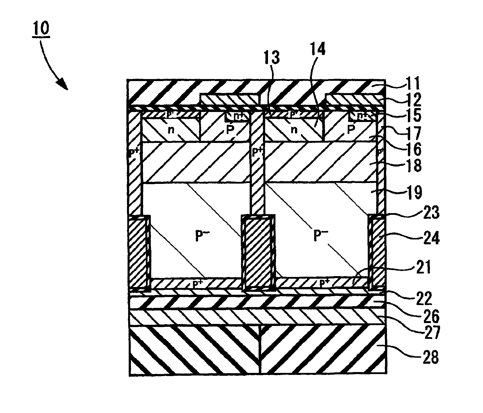
[0056]In the image pickup device 10 of the embodiment, the structure of light blocking members 35 which are formed as an embedded member on the silicon oxide film 26, and the configuration of an epitaxial layer in the periphery of the light blocking members 35 are different from those of the Hereinafter, different portions will be described.

[0057]As shown in FIG. 6, the light blocking members 35 made of a metal material or the like are formed in boundaries of adjacent pixels on the surface of the silicon oxide film 26. The light blocking members 35 are covered by a p+ type epitaxial layer 31 having a high impurity concentration. The layer covering the light blocking members 35 is not restricted to the epitaxial layer 31, and may be configured by another epitaxial layer or an impurity diffusion layer as far as it is a non-depleted layer which does not generate charges in boundaries to the light blocking members 35. The light blocking members 35 are connected to a grounding circuit s...

third embodiment

[0058]FIG. 7 shows the image pickup device of the invention. The image pickup device 10 of the embodiment has a configuration where the light blocking members 24 extend toward the surface side in the vertical direction (the upward and downward direction in FIG. 7) of the photoelectric converting layer. Specifically, the light blocking members 24 formed on the upper face of the silicon layer 22, and the insulating film 23 formed outside the light blocking members 24 are formed in a state where they extend toward the surface side of the photoelectric converting layer, surface-side end portions come into contact with or approach rear face-side end portions. According to the configuration, light which is incident on the photoelectric converting layer can be prevented by the light blocking members 24 from entering surrounding pixel regions, and occurrence of color mixture can be suppressed.


PUM


Abstract

An image pickup device including a semiconductor substrate that is irradiated with light from a first surface side thereof, and reading signal charges generated in the semiconductor substrate in accordance with the light from a second surface side thereof, wherein the semiconductor substrate includes: a photoelectric converting layer that includes a plurality of impurity diffusion layers on the second surface side of the semiconductor substrate, and that produces the signal charges by photoelectric conversion; and an embedded member that includes a light blocking material, and that is embedded in an impurity diffusion layer on a surface side of the photoelectric converting layer, the surface side facing the second surface side of the semiconductor substrate.

Description

BACKGROUND OF THE INVENTION[0001]1. Field of the Invention[0002]The present invention relates to an image pickup device which photoelectrically converts incident light to produce signal charges, and more particularly to an image pickup device in which color mixture can be reduced, a method of producing such an image pickup device, and a semiconductor substrate for such an image pickup device.[0003]2. Background Art[0004]As shown in ITE Technical Report vol. 30, No. 25, pp. 25-28 “Rimen Shosya CMbS Image Sensor,” U.S. Pat. No. 5,828,088, Japanese Patent No. 3,722,367 and JP-A-2005-150463 (the term “JP-A” as used herein means an “unexamined published Japanese patent application”), a solid-state image pickup device of the backside illumination type, which has been used only in a specific application field where emphasis is placed on the quantum efficiency or the aperture ratio, has been proposed to be used in a consumer image pickup device such as a digital camera or a digital video ca...

Claims


Application Information

Patent Timeline
Patent Type & Authority Patents(United States)
IPC IPC(8): H04N3/14H01L27/14
CPCH01L27/14623H01L27/1464H01L27/14687H01L27/14603H01L27/14643H01L27/1463
Inventor UYA, SHINJI
Owner FUJIFILM CORP
Why Eureka
Try Eureka