Method for manufacturing photoelectric transducer, and electronic apparatus

a technology of photoelectric transducers and electronic devices, which is applied in the manufacture of final products, instruments, optical radiation measurement, etc., can solve the problems of difficult to obtain a silicon film with the method of coating composites being applied on the substrate is not suitable, and the thickness of the film thickness is difficult to obtain. achieve the effect of high photoelectric conversion efficiency, low cost and thick droplet thickness

Inactive Publication Date: 2006-09-28
SEIKO EPSON CORP
View PDF21 Cites 4 Cited by
  • Summary
  • Abstract
  • Description
  • Claims
  • Application Information

AI Technical Summary

Benefits of technology

[0010] An advantage of the invention is to provide a method in which a micron-order I type semiconductor layer required for solar batteries of a PIN structure is manufactured at low cost using a liquid silicon material.
[0011] According to an aspect of the invention, a method for manufacturing a photoelectric transducer includes the steps of forming a first electrode on a substrate; forming a first semiconductor layer of a P type or an N type on the first electrode; forming a second semiconductor layer of an I type on the first semiconductor layer; forming a third semiconductor layer of an N type or a P type on the second semiconductor layer; and forming a second electrode on the third semiconductor layer. In the method, when the first semiconductor layer is made to be a P type, the third semiconductor layer is made to be an N type, and when the first semiconductor layer is made to be an N type, the third semiconductor layer is made to be a P type, wherein the step of forming the second semiconductor layer includes the steps of: forming a precursor film of the silicon film on the first semiconductor layer by arranging droplets containing a silicon compound in an island shape; and converting the precursor film into a silicon film by carrying out heat treatment or photoirradiation treatment to the precursor film.
[0012] If the liquid containing a silicon compound is arranged as a substantially hemispherical droplet in an island shape on the first semiconductor layer, it is possible to form a film thicker than in the case where the coating film is formed in a wide area with a spin coating method or the like. As for the substantially semi-sphere droplet, although the thickness thereof becomes thin due to the influence that solvent and hydrogen escape in the subsequent heating or photoirradiation step, the micron-order semiconductor thin film can be obtained. In such a semiconductor thin film, cracks hardly occur and the film also hardly peels off from the substrate.
[0013] It is preferable to include the step of forming a liquid-repellent film in regions other than the region, in which the droplets containing a silicon compound are to be arranged, in the first semiconductor layer prior to forming the second semiconductor layer.
[0014] If a liquid-repellent / lyophilic pattern is formed in the surface of the first semiconductor layer prior to arranging the droplets containing a silicon compound, the droplets will remain in the lyophilic region and will not get wet and not spread to the liquid-repellent region. Consequently, it is possible to arrange more droplets in the lyophilic region and make the thickness of the droplet thicker.
[0015] Moreover, it is preferable that the thickness of the silicon film be 1 μm or more after the step of heat treatment or photoirradiation treatment. By setting the film thicknesses of the I type semiconductor layer to 1 μm or more, preferably 2 μm or more, a photoelectric transducer with a high photoelectric-conversion efficiency and high performance can be obtained.

Problems solved by technology

For this reason, the method for applying the coating composite onto a substrate is not suitable, and the forming is usually carried out with a relatively costly method such as CVD.
If the contact angle is 40 degrees or less, the sufficient droplets can not be arranged in the lyophilic region, and it becomes difficult to obtain a silicon film with a necessary film thickness.
Moreover, if the contact angle is 120 degrees or more, the adhesion force may become weak when forming the third semiconductor layer.

Method used


Image

  • Method for manufacturing photoelectric transducer, and electronic apparatus
  • Method for manufacturing photoelectric transducer, and electronic apparatus
  • Method for manufacturing photoelectric transducer, and electronic apparatus

Examples


first embodiment

[0036] First Embodiment

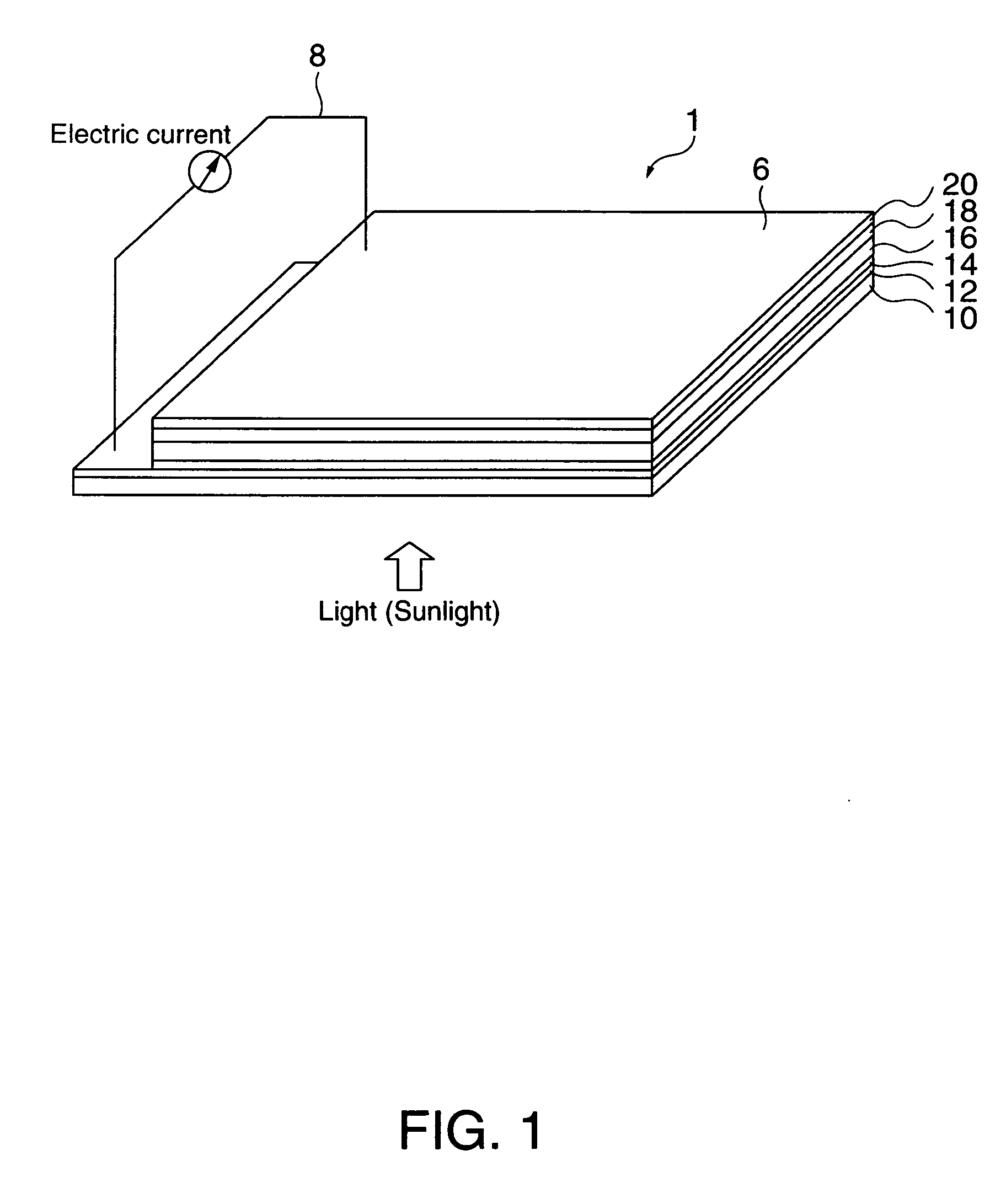
[0037]FIG. 1 is a perspective view showing an embodiment of the photoelectric transducer of the invention. In addition, in the following description, on the space of FIG. 1 the upper side is referred to as the “upper” or “top”, and the lower side is referred to as the “lower” or “bottom”, and the upper side face of each layer (each member) is referred to as the “upper face” and the lower side face is referred to as the “lower face”.

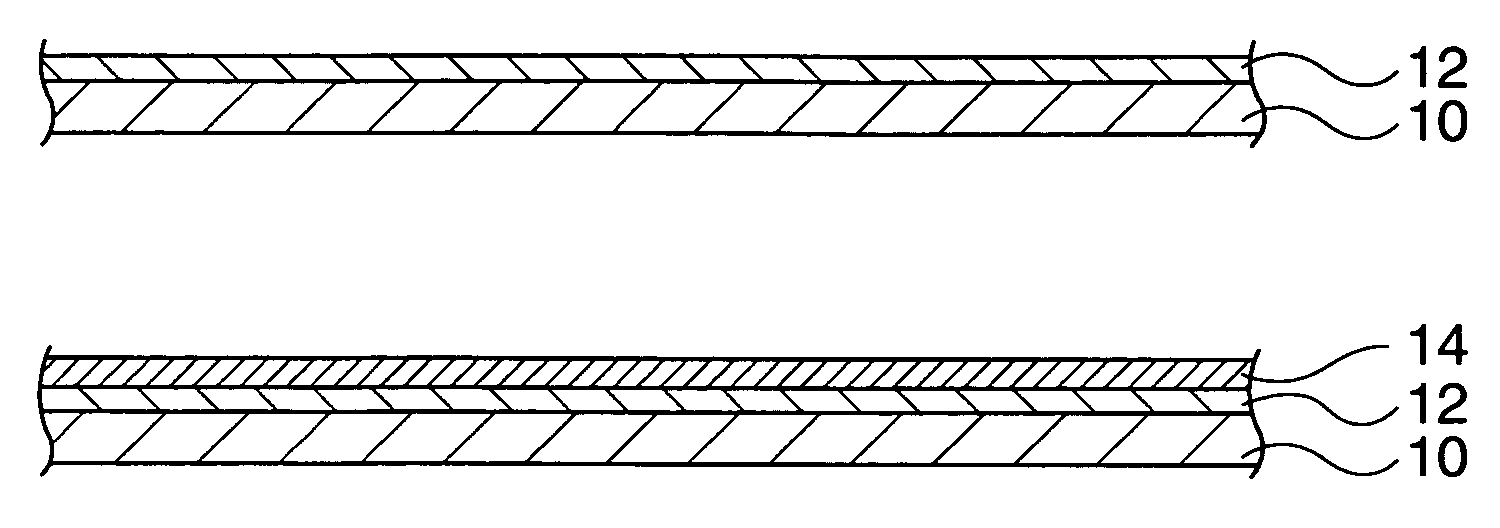
[0038] A photoelectric transducer 1 shown in FIG. 1 is the so-called dry type photoelectric transducer, which does not require an electrolytic solution. This photoelectric transducer 1 includes a substrate 10, a first electrode (a plate electrode) 12, a P type semiconductor layer 14 as a first semiconductor layer, an I type semiconductor layer 16 as a second semiconductor layer, an N type semiconductor layer 18 as a third semiconductor layer, and a second electrode (an opposing electrode) 20. Hereinafter, the configuration of each ...

second embodiment

[0072] Second Embodiment

[0073] This embodiment features that after forming the island-like silicon film as the I type semiconductor layer, droplets containing a silicon compound are arranged offsetting the center thereof relative to that of the already-formed silicon film, thereby forming a thicker I type semiconductor layer.

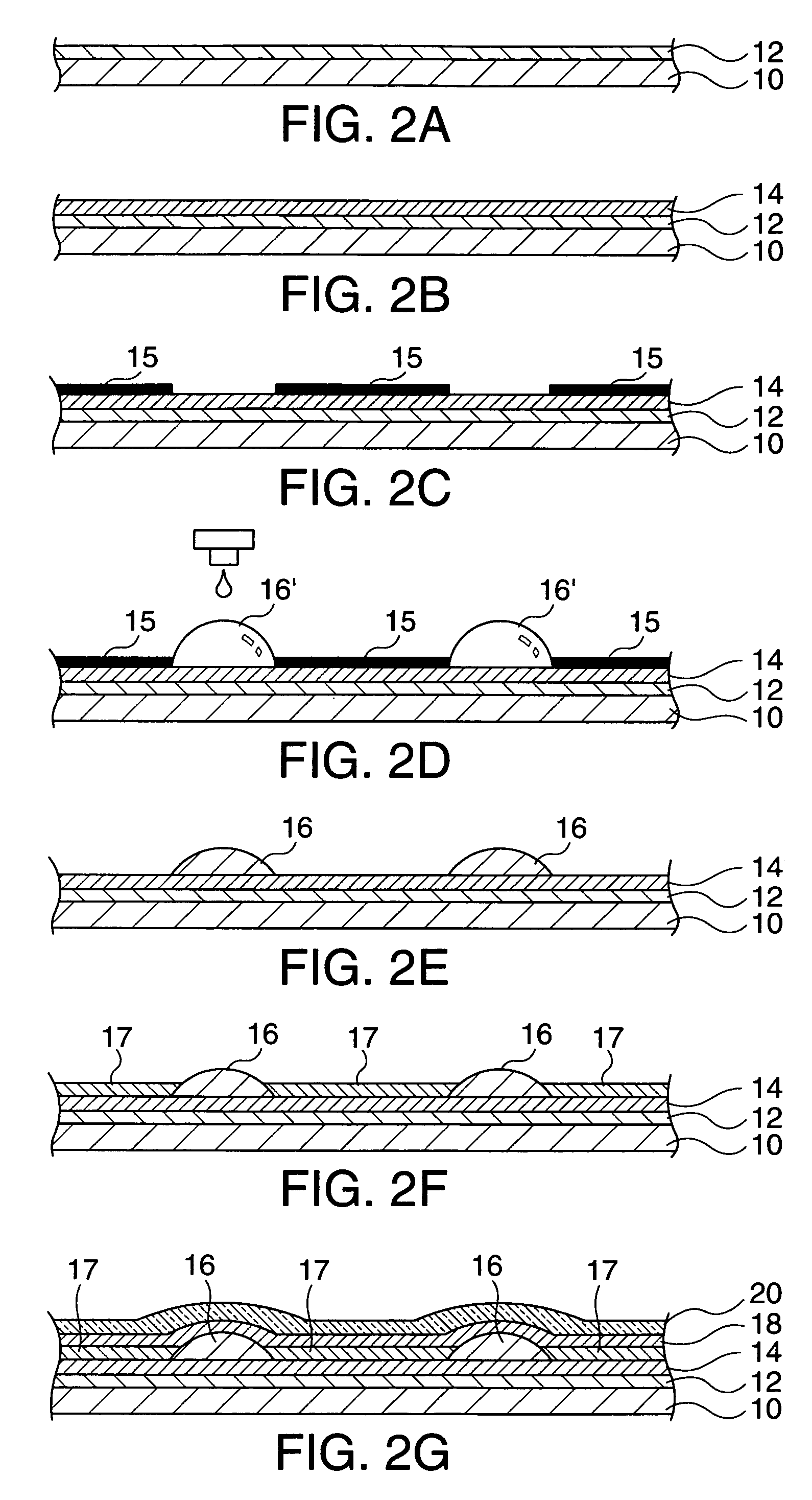
[0074] After having proceeded to the step of forming the first electrode, the step of forming the P type semiconductor layer, the step of forming the liquid-repellent film, the step of forming the precursor film of the silicon film, and the heat treatment step, a silicon film, which is the I type semiconductor layer, is formed in an island shape. In FIG. 4A, there is shown a part of the plane view in the state in which the island-like silicon film is formed, and a sectional view along the VA through VA line in the view is shown in FIG. 5A.

[0075] Step of Forming the Liquid-Repellent Film: A Second Time

[0076] Then, as shown in FIG. 4B, and FIG. 5B which is a se...


PUM


Abstract

A method for manufacturing a photoelectric transducer, comprising: forming a first electrode on a substrate; forming a first conductivity-type semiconductor layer on the first electrode; forming an I type semiconductor layer on the first conductivity-type semiconductor layer; forming on the I type semiconductor layer a second conductivity-type semiconductor layer that is different from the first conductivity-type; and forming a second electrode on the second conductivity-type semiconductor layer, wherein the forming of the I type semiconductor layer includes: forming a precursor film of the I type semiconductor layer on the first conductivity-type semiconductor layer by arranging droplets containing a silicon compound in an island shape; and converting the precursor film into the I type semiconductor layer by carrying out heat treatment or photoirradiation treatment to the precursor film.

Description

BACKGROUND [0001] 1. Technical Field [0002] The present invention relates to a method for manufacturing a photoelectric transducer using a liquid containing a silicon compound, and to an electronic apparatus provided with the photoelectric transducer manufactured with this method. [0003] 2. Related Art [0004] Conventionally, as an environment-friendly power supply, photoelectric transducers such as a solar battery have been attracting the attention, and single crystal silicon type solar batteries used for satellite batteries or the like, and solar batteries using polycrystal silicon or amorphous silicon are widely used for industries and homes. [0005] The amorphous-silicon solar battery typically has a structure, the so-called PIN structure, in which a first conductivity-type semiconductor layer and a second conductivity-type semiconductor layer (e.g., a P type semiconductor layer and an N type semiconductor layer) sandwich a light absorption layer composed of an I type semiconducto...

Claims


Application Information

Patent Timeline
Patent Type & Authority Applications(United States)
IPC IPC(8): G01J1/42
CPCH01L31/077H01L31/1872H01L31/202Y02E10/50Y02E10/546Y02P70/50
Inventor FURUSAWA, MASAHIROYUDASAKA, ICHIOTANAKA, HIDEKIMIYAMOTO, TSUTOMUSHIMAMURA, HIDEO
Owner SEIKO EPSON CORP
Why Eureka
Try Eureka