Quasicrystalline structures and uses thereof

a technology of crystalline structures and crystalline structures, applied in the field of crystalline structures, can solve problems such as dielectric breakdown, short channel effects, and hot carriers

Active Publication Date: 2011-11-22
THE TRUSTEES FOR PRINCETON UNIV
View PDF6 Cites 16 Cited by
  • Summary
  • Abstract
  • Description
  • Claims
  • Application Information

AI Technical Summary

Benefits of technology

[0017]In some embodiments, the invention relates to a waveguide comprising a photonic quasicrystal that can guide incoming light at any angle. In further embodiments, the invention relates to a waveguide comprising a photonic quasicrystal formed on the top of a light emitting diode. In further embodiments, the photonic quasicrystal may guide light entering the photonic quasicrystal from any direction.
[0051]It is also a further object of certain embodiments of the invention to provide an improved system and method for constructing photonic stopgap structures which can be switched from one structural state to another state by repositioning particles to thereby modify physical and / or chemical properties of the arrangement.

Problems solved by technology

Further miniaturization introduces several technological problems such as dielectric breakdown, hot carriers, and short channel effects.

Method used


Image

  • Quasicrystalline structures and uses thereof
  • Quasicrystalline structures and uses thereof
  • Quasicrystalline structures and uses thereof

Examples


example 1

Stereolithography Created Lattices

[0120]A D-dimensional periodic lattice has D integer independent basis vectors, while D+N integer linearly independent vectors (with integer N≧1) are required to describe the quasicrystal lattice. The icosahedral quasicrystal lattice of points can be constructed by projecting the points of a six-dimensional hypercubic lattice, the six-dimensional analog of a three-dimensional cubic lattice. The coordinate of any lattice point can be described by the relation:

[0121]R=∑i=16⁢ni⁢ai,

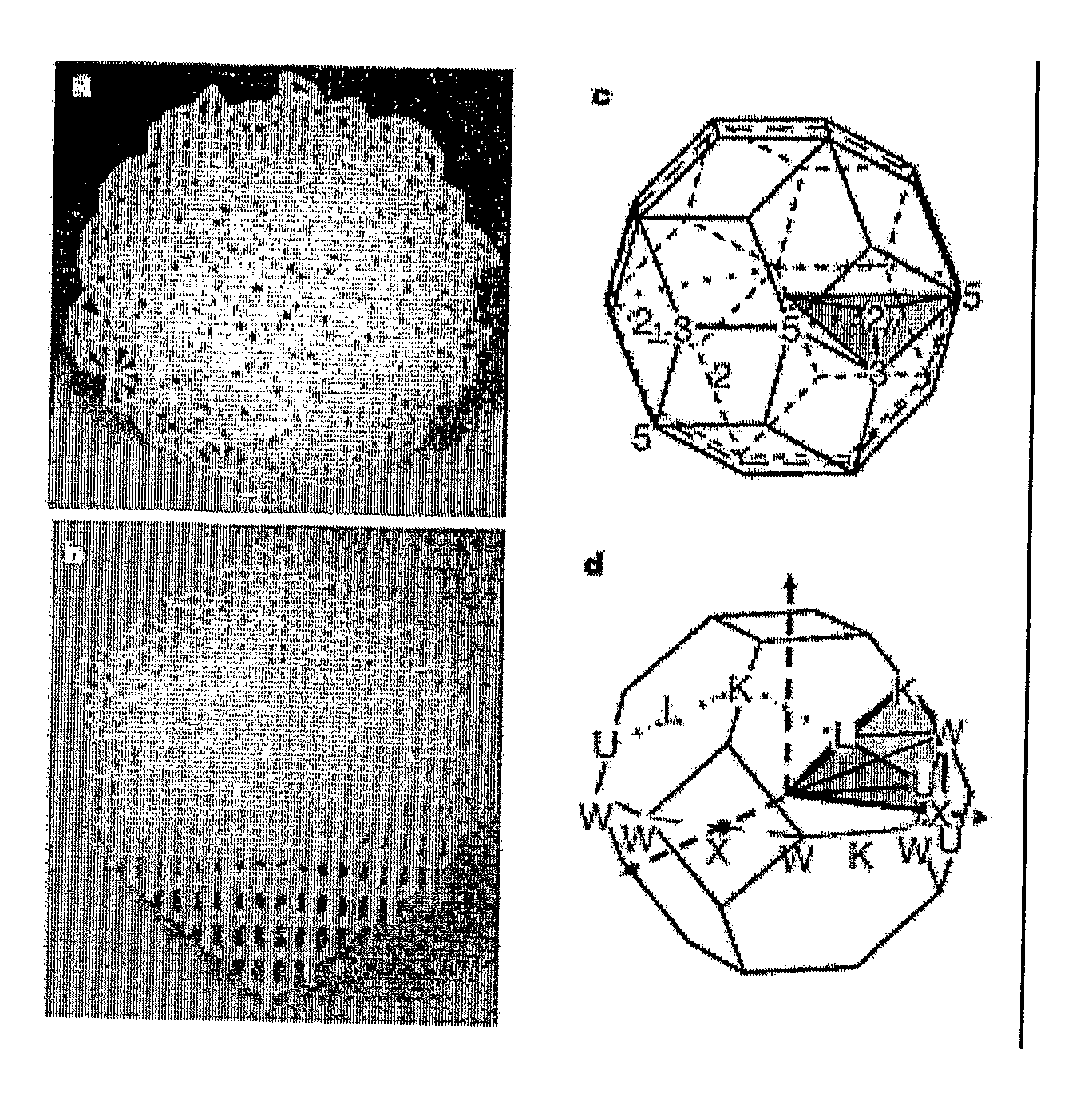
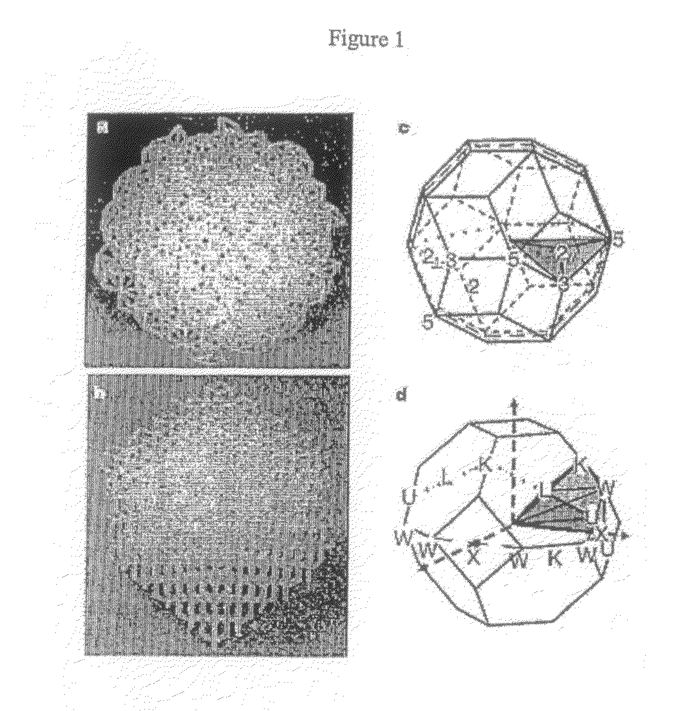
where the ni are a subset of the integers and ai are the 6 basis vectors: a1=(1,τ,0), a2=(−1,τ,0), a3=(0,1,τ), a4=(0,−1,τ), a5=(τ,0,1), a6=(τ,0,−1), and τ=(√5−1) / 2 the golden mean. The structure has twelve 5-fold, fifteen 3-fold and thirty 2-fold symmetry axes. The lattice points of the icosahedral structure are generated and a solid structure created by using equal length rods to connect points in pairs. The overall shape shown in FIG. 1a is a dodecahedron, so that each of t...

example 2

Transmission Measurements

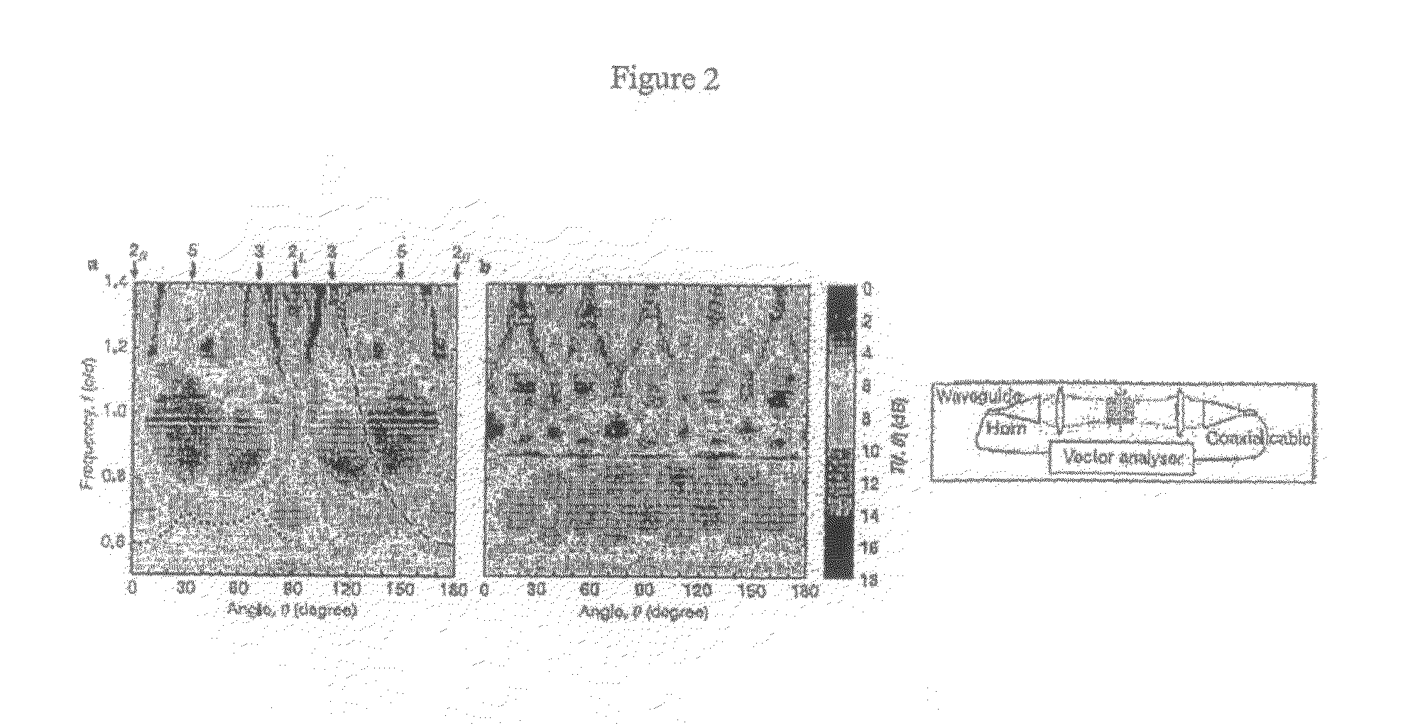
[0123]Transmission measurements for the icosahedral quasicrystal of FIG. 1a can be made with a HP Model 8510C Vector Analyzer in three bands, from 8 to 15, from 15 to 26 and from 26 to 42 GHz. To approximate plane waves, a single TE10 mode is coupled through two sets of horn-attached waveguides with two custom-made polystyrene microwave lenses as schematically shown in the insert in FIG. 2. Before the sample is put in, the transmission spectrum of the setup is recorded for normalization. Since the sample has different symmetry and dimensions in different directions, the transmission spectrum should be orientation and polarization sensitive. The sample is aligned so that the incident beam is perpendicular to one of the sample's rotational symmetry axes. The sample is rotated along that rotational symmetry axis, and the relative transmission spectrum is recorded, for example, every 2 degrees. For the quasicrystal, a rotation about the 2-fold axis covers all th...

example 3

Holographic Optical Trapping

[0124]The foregoing photonic quasicrystal is macroscopic, however, this design can be miniaturized, e.g., for nanoparticles or other particles. For example, laser tweezers can be used for particle trapping or two-photon polymerization can be used. Such methods allow construction of a quasicrystalline matrix of dielectric components with a photonic bandgap in the visible.

[0125]Computer generated holograms are projected through a high-numerical-aperture microscope objective lens to create large three-dimensional arrays of optical traps. Light at 532 nm form a frequency-doubled diode-pumped solid state laser (Coheret Verdi) is imprinted with phase-only holograms using a liquid crystal spatial light modulator (SLM) (Hamamatsu X8267 PPM). The modified laser beam is relayed to the input pupil of a 100×NA 1.4 SPlan Apo oil immersion objective mounted in an inverted optical microscope (Nikon TE-2000U), which focuses it into traps. The same objective lens is used ...


PUM

PropertyMeasurementUnit
lengthaaaaaaaaaa
wavelengthsaaaaaaaaaa
diameteraaaaaaaaaa

Abstract

This invention relates generally to the field of quasicrystalline structures. In preferred embodiments, the stopgap structure is more spherically symmetric than periodic structures facilitating the formation of stopgaps in nearly all directions because of higher rotational symmetries. More particularly, the invention relates to the use of quasicrystalline structures for optical, mechanical, electrical and magnetic purposes. In some embodiments, the invention relates to manipulating, controlling, modulating and directing waves including electromagnetic, sound, spin, and surface waves, for a pre-selected range of wavelengths propagating in multiple directions.

Description

[0001]This application claims the benefit of U.S. Provisional Application No. 60 / 697,829, filed Jul. 8, 2005 and U.S. Provisional Application No. 60 / 697,872, filed Jul. 8, 2005.GOVERNMENT RIGHTS[0002]This invention was made with government support under DMR0213706 and DMR0243001, and DE-FG02-91ER40671 awarded by the National Science Foundation and the Department of Energy respectively. The government may have certain rights in the invention.FIELD OF THE INVENTION[0003]This invention relates generally to the field of quasicrystalline structures. In preferred embodiments, the stopgap structure is more spherically symmetric than periodic structures facilitating the formation of stopgaps in nearly all directions because of higher rotational symmetries. More particularly, the invention relates to the use of quasicrystalline structures for optical, mechanical, electrical and magnetic purposes. In some embodiments, the invention relates to manipulating, controlling, modulating and directin...

Claims


Application Information

Patent Timeline
Patent Type & Authority Patents(United States)
IPC IPC(8): G02F1/00
CPCB82Y20/00B82Y30/00G02B6/1225H01L33/002C08F222/385C08G65/22B33Y80/00C08F220/56C08G59/245
Inventor STEINHARDT, PAUL JOSEPHCHAIKIN, PAUL MICHAELMAN, WEINING
Owner THE TRUSTEES FOR PRINCETON UNIV
Why Eureka
Try Eureka