

High performance CMOS devices and methods for making same
a complementary metal oxide semiconductor and high-performance technology, applied in the direction of semiconductors, semiconductor devices, electrical apparatus, etc., can solve the problems of difficult low junction leakage current, and the dimension of the cmos device must be scaled down, so as to achieve good short channel effects and low parasitic junction capacitance , the effect of high performance cmos
- Summary
- Abstract
- Description
- Claims
- Application Information
AI Technical Summary
Benefits of technology
Problems solved by technology
Method used
Image

Examples
Embodiment Construction
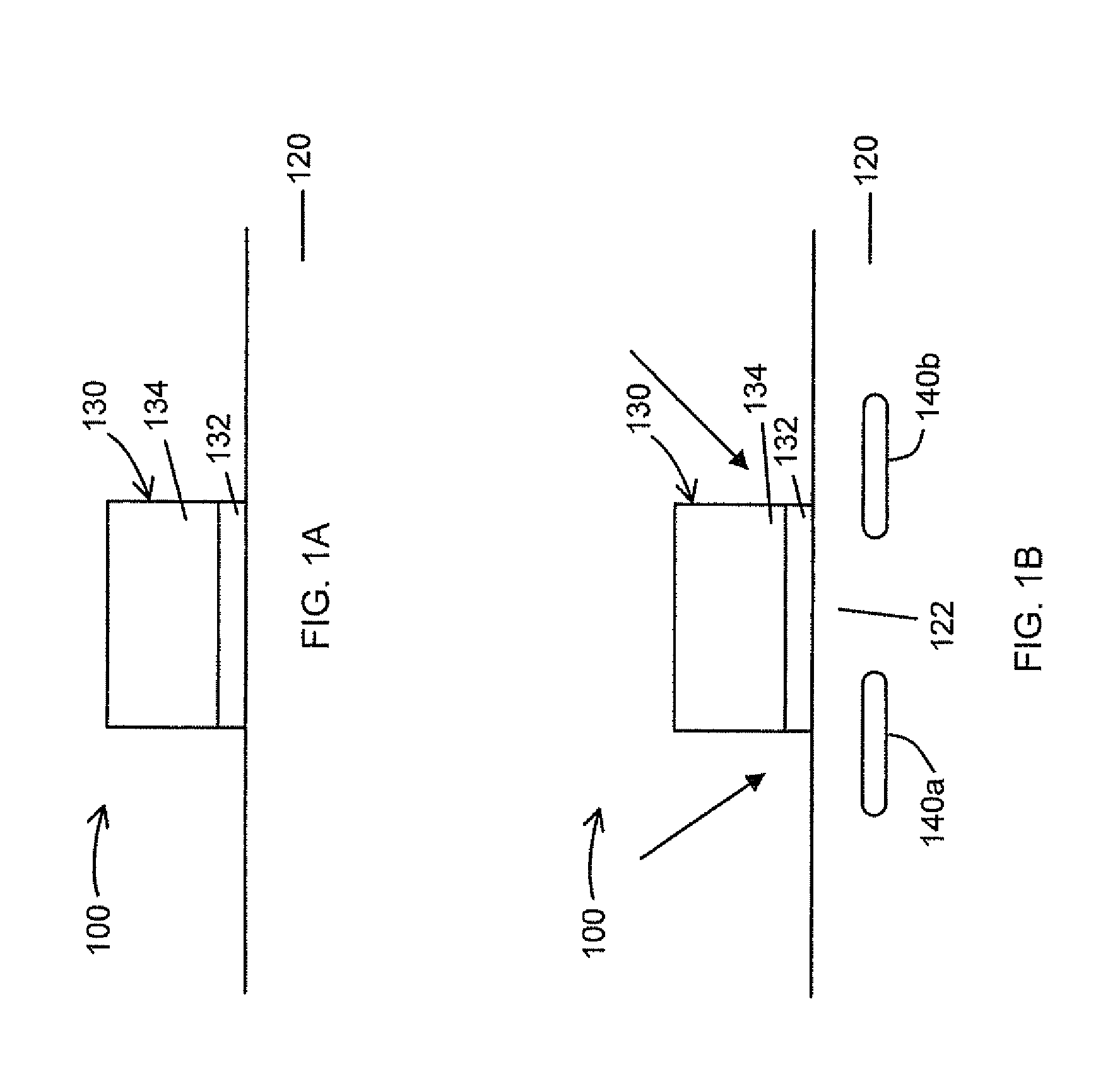
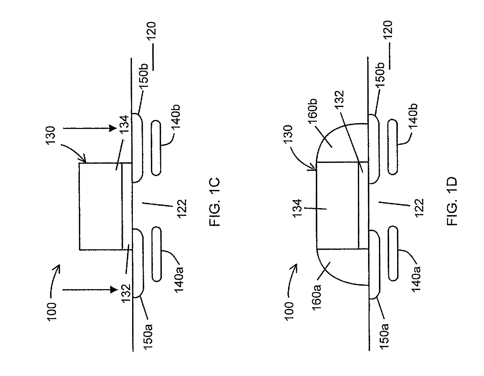
[0017]FIGS. 1A-1E are sectional views illustrating a method of fabricating a scaled down transistor 100 (e.g. PMOS or NMOS) of a high performance CMOS device according to the present invention. As illustrated in FIG. 1A, the method commences with the formation of a gate structure 130 over a substrate 120. The substrate 120 is not limited to a particular type and may be include, without limitation, an element semiconductor, such as Si and Ge, or a compound semiconductor, such as GaAs, InGaAs and ZnSe. The gate structure 130 may include a gate oxide 132, such as SiO2, disposed over the substrate 120 and a gate conductor 134, such as poly-Si, poly SiGe, a metal, a metal oxide, a metal nitride, a silicide and combinations thereof, disposed over the gate oxide 132. The gate structure 130 may be formed using conventional methods well known in the art.
[0018]As illustrated in FIG. 1B, a self-aligning pocket ion implantation process is performed to form self-aligned first and second pocket i...
PUM
 Abstract
Description
Claims
Application Information