Method for manufacturing substrate having built-in components

a technology of built-in components and substrates, which is applied in the direction of sustainable manufacturing/processing, final product manufacturing, printed circuit non-printed electric components association, etc., can solve the problems of high probability of solder flow, short circuit, and reliability problems, and achieve the effect of preventing short circui

Active Publication Date: 2011-12-06
MURATA MFG CO LTD
View PDF96 Cites 8 Cited by
  • Summary
  • Abstract
  • Description
  • Claims
  • Application Information

AI Technical Summary

Benefits of technology

To overcome the problems described above, preferred embodiments of the present invention provide a method for manufacturing a highly reliable substrate having built-in components which can prevent a short circuit caused by the spread of solder or conductive adhesive.
According to preferred embodiments of the present invention, the land regions and the wetting prevention region surrounding the land regions are formed on one primary surface of the metal foil, the terminal electrodes of the circuit component are connected to the land regions using solder or conductive adhesive, and the resin layer is formed on the metal foil and the circuit component. Accordingly, the spread of solder or conductive adhesive can be restricted by the wetting prevention region, and further, the overall amount of solder or conductive adhesive used can be decreased as compared to that of a conventional method in which an insulating layer is used. Thus, the risk of generating solder flow and a short circuit can be greatly reduced. In addition, in the case of a conventional method in which an insulating layer and a resin layer are made of different materials, an adhesion strength at a dissimilar interface therebetween decreases, and as a result, problems such as solder flow may occur. However, in preferred embodiments of the present invention, since no insulating layer is required, the problems as described above are avoided.

Problems solved by technology

However, in the manufacturing method described above, when the circuit components are mounted, or the resin sheet is pressure bonded, since the conductive adhesives are spread in a primary surface direction of the metal foil, the conductive adhesives are brought into contact with each other or are brought into contact with adjacent wiring patterns, so that a short circuit may occur.
The same problem also occurs when a solder is used instead of the conductive adhesive.
In particular, when a solder is used, since the amount thereof is large, solder flow is very likely to occur, and thus, a reliability problem may arise.

Method used


Image

  • Method for manufacturing substrate having built-in components
  • Method for manufacturing substrate having built-in components
  • Method for manufacturing substrate having built-in components

Examples


first preferred embodiment

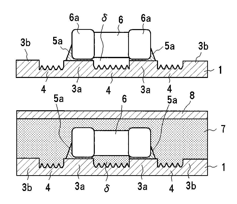
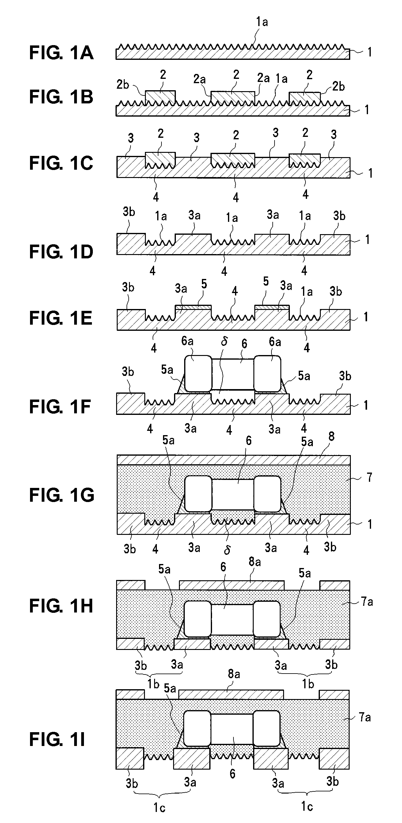
Hereinafter, a first preferred embodiment of a method for manufacturing a substrate having built-in components according to the present invention will be described with reference to FIGS. 1A to 1I. In order to simplify the illustration, FIGS. 1A to 1I show a portion of a manufacturing process of a substrate having built-in components in which only one circuit component is included. However, an actual substrate having built-in components includes a plurality of circuit components. Furthermore, in an actual manufacturing process, a substrate having built-in components is made in a mother substrate state and is then individually obtained therefrom by cutting the mother substrate.

FIG. 1A shows a first step in which a metal foil 1 having a rough surface 1a formed entirely or substantially entirely at one primary surface side is prepared. The metal foil 1 is processed in a subsequent eighth step which will be described later, so that a wiring pattern is formed on one surface of the substr...

second preferred embodiment

Next, a second preferred embodiment of the method for manufacturing a substrate having built-in components according to the present invention will be described with reference to FIGS. 4A to 4J.

FIG. 4A shows a first step in which an oxide film 11a is formed entirely or substantially entirely on one primary surface of a metal foil 11. A material and a thickness of the metal foil 11 are substantially the same as those in the first preferred embodiment. As a method for forming the oxide film 11a, any method, such as a thermal treatment or a chemical treatment, for example, may preferably be used. In this example, although the oxide film 11a is formed on a flat surface of the metal foil 11, a roughened metal foil surface as shown in FIG. 1 may be processed by an oxidation treatment.

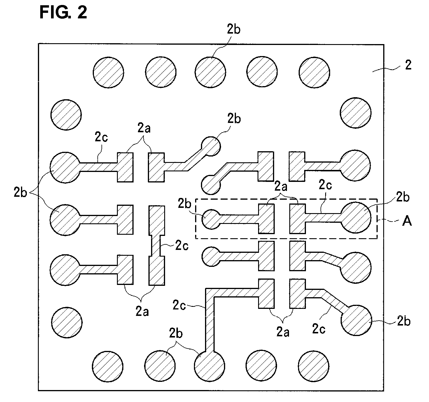
FIG. 4B shows a second step in which a plating resist 12 is pattern-formed on the oxide film 11a of the metal foil 11. A material and a pattern forming method of the plating resist 12 are substantially the sam...

third preferred embodiment

Next, a third preferred embodiment of the method for manufacturing a substrate having built-in components according to the present invention will be described with reference to FIGS. 5A to 5I. Since steps shown in FIG. 5A to 5C are substantially the same as those shown in FIG. 1A to 1C, the same reference numerals as those in FIGS. 1A to 1C are used, and a description is omitted.

In a step shown in FIG. 5D, Sn or Sn-alloy plating is preferably performed on the surface of the metal foil 1 on which the plating resist 2 is formed, so that pre-coat layers 20 are formed. In this example, since the land regions 3a and the wiring regions 3b are exposed through the opening portions of the plating resist 2, the pre-coat layers 20 are formed on the regions. As the Sn alloy, for example, Sn—Ag, Sn—Bi, Sn—Ag—cu, and other suitable Sn alloys may preferably be used. As a plating method, any suitable method, such as an electroless plating method or an electroplating method, for example, may prefera...


PUM

PropertyMeasurementUnit
thicknessaaaaaaaaaa
surface roughness Rzaaaaaaaaaa
thicknessaaaaaaaaaa

Abstract

A method for manufacturing a substrate having built-in components prevents a short circuit caused by the spread of solder or conductive adhesive. Land regions to connect a circuit component and a wetting prevention region surrounding the land regions are formed on one primary surface of a metal foil. Terminal electrodes of the circuit component are electrically connected to the land regions using solder, and an uncured resin is disposed on and pressure bonded to the metal foil and the circuit component, so that a resin layer in which the circuit component is embedded is formed. Subsequently, a wiring pattern is formed by processing the metal foil. The wetting prevention region is a region obtained by roughening or oxidizing one primary surface of the metal foil so as to reduce solder wettability.

Description

BACKGROUND OF THE INVENTION1. Field of the InventionThe present invention relates to a method for manufacturing a substrate having built-in components in which at least one circuit component is embedded in a resin layer.2. Description of the Related ArtRecently, as a result of the trend toward reducing the size of electronic apparatuses, a reduction in the size of circuit substrates which are used to mount circuit components, such as a chip capacitor, has been required. In response, the reduction in the size of circuit substrates has been achieved by embedding circuit components in a circuit substrate to form a module so that the mounting areas of the circuit components are reduced. Since a substrate having built-in components in which circuit components are embedded in a resin substrate is lightweight and is not subjected to high temperature firing, unlike a ceramic substrate, there is an advantage in that the type of circuit component to be embedded in the substrate is not particu...

Claims


Application Information

Patent Timeline
Patent Type & Authority Patents(United States)
IPC IPC(8): H05K3/30H01R43/00H05K7/00H05K1/18H05K1/00H05K13/00H05K3/20
CPCH05K1/187Y10T29/49169H05K3/243H05K3/3442H05K3/3452H05K3/382H05K2201/0355H05K2201/10636H05K2201/2081H05K2203/0307H05K2203/0315H05K2203/1152Y10T29/49142Y10T29/49128Y10T29/49171Y10T29/49146Y10T29/4913H05K3/205Y02P70/50
Inventor HIRAYAMA, KATSURONISHIMURA, SHIGEO
Owner MURATA MFG CO LTD
Why Eureka
Try Eureka