Connector for implementing multi-faceted interconnection and manufacturing method thereof

a technology of interconnection and connector, applied in the direction of semiconductor devices, semiconductor/solid-state device details, electrical apparatus, etc., can solve the problems of occupying a vast available space, affecting the use of space, so as to avoid mechanical cutting and improve the utilization rate of space, the effect of shortening the electric transmission path

Active Publication Date: 2022-03-03
ZHUHAI ADVANCED CHIP CARRIERS & ELECTRONICS SUBSTRATE SOLUTIONS TECH
View PDF1 Cites 1 Cited by
  • Summary
  • Abstract
  • Description
  • Claims
  • Application Information

AI Technical Summary

Benefits of technology

[0012]The embodiment of the invention aims to solve the technical problem, and provides a connector for implementing multi-faceted interconnection and a manufacturing method thereof. According to the invention, the multi-facete

Problems solved by technology

With the development of industry, people expect more and more diversified functions as well as lighter, thinner and smaller properties of consumer electronic products, which requires the electronic products to be packaged denser, and packaged more thinner and smaller individually, and reduced size, in addition, poses great challenges to processes and devices.
Only bonding wires can be used for realizing the electrical connection between different devices in the “X” and “Y” directions at present, however, the bonding wires are long, the electrical transmission path is long, the cost is high, and the bonding wires must be of a certain radian, which undoubtedly takes up vast available space.
Even if a wafer-level cutting apparatus is used, single products will be produced by cutting since it is impossible to jump, and subsequent processes, such as the manufacture of protective layers of sidewalls and surfaces, cannot be completed.
In addition, the cutting blades are commonly made of high-speed steel, hard alloy materials, diamond and the like, the cutting blades are used for cutting copper metals, the abra

Method used


Image

  • Connector for implementing multi-faceted interconnection and manufacturing method thereof
  • Connector for implementing multi-faceted interconnection and manufacturing method thereof
  • Connector for implementing multi-faceted interconnection and manufacturing method thereof

Examples


Embodiment Construction

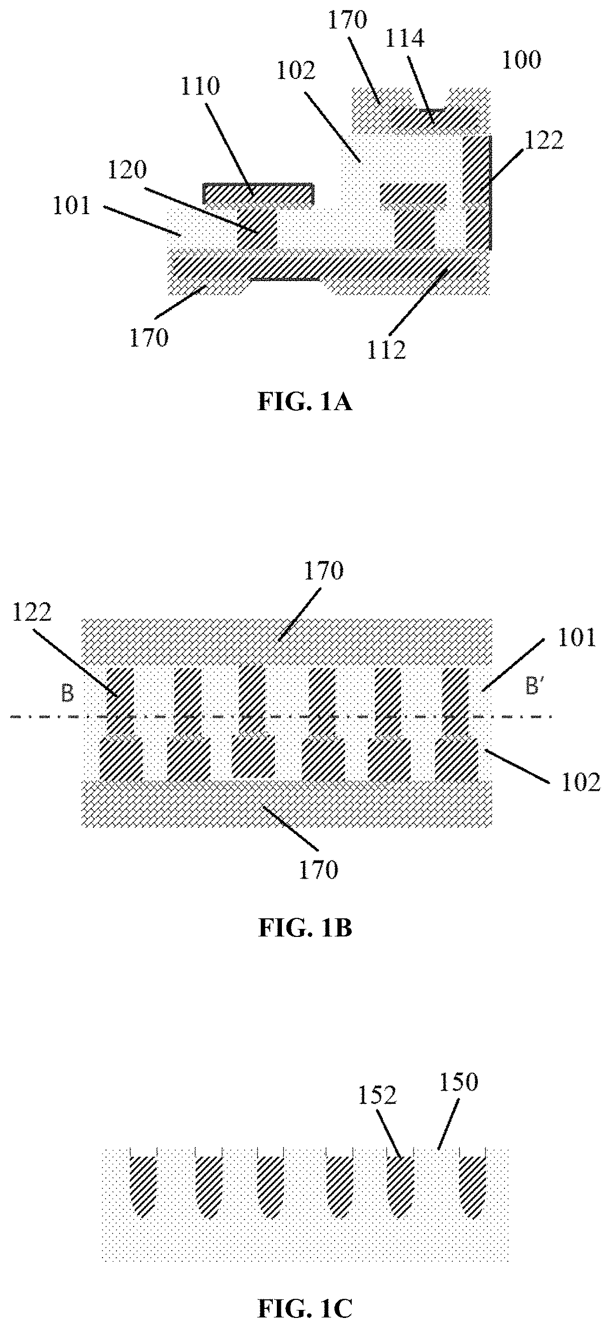
[0092]Referring to FIG. 1A, a cross-sectional view of a connector 100 implementing a multi-faceted interconnection is shown. The connector 100 includes: a first dielectric layer 101 between a first circuit layer 110 and a second circuit layer 112; a first copper pillar layer 120 connecting the first circuit layer 110 and the second circuit layer 112 in the first dielectric layer 101; a second dielectric layer 102 on the first circuit layer 110; a third circuit layer 114 on the second dielectric layer 102; and a vertical second copper pillar layer 122 connecting the third circuit layer 114, wherein an opening is formed in the second dielectric layer 102 to expose the first circuit layer 110, and the second copper pillar layer 122 is exposed to the side faces of the side end faces of the first dielectric layer 101 and the second dielectric layer 102. A solder mask 170 is formed on the second circuit layer 112 and the third circuit layer 114. The connector 100 may be side-electrically ...


PUM


Abstract

A connector for implementing multi-faceted interconnection according to an embodiment of the present disclosure includes a first dielectric layer between a first circuit layer and a second circuit layer, a first copper pillar layer connecting the first circuit layer and the second circuit layer in the first dielectric layer, a second dielectric layer on the first circuit layer, a third circuit layer on the second dielectric layer, and a vertical second copper pillar layer connected to the third circuit layer, wherein an opening is formed in the second dielectric layer to expose the first circuit layer, and the second copper pillar layer exposes side faces facing side end faces of the first dielectric layer and the second dielectric layer.

Description

CROSS-REFERENCE TO RELATED APPLICATION[0001]This application claims the benefit under 35 USC § 119(a) of Chinese Patent Application No. 202010911278.X, filed on Sep. 2, 2020, in the China Intellectual Property Office, the entire disclosure of which is incorporated herein by reference for all purposes.BACKGROUND1. Technical Field[0002]The invention relates to an electronic device packaging structure, in particular to a connector structure of a multi-faceted interconnection which plays a connecting role in a semiconductor package and a manufacturing method thereof.2. Background of the Invention[0003]With the development of industry, people expect more and more diversified functions as well as lighter, thinner and smaller properties of consumer electronic products, which requires the electronic products to be packaged denser, and packaged more thinner and smaller individually, and reduced size, in addition, poses great challenges to processes and devices. However, different packages in...

Claims


Application Information

Patent Timeline
IPC IPC(8): H01L23/532H01L23/538H01L23/00
CPCH01L23/53228H01L24/14H01L23/5386H01L23/49822H01L23/49838H01L23/49805H01L23/5383H01L21/4857H01L23/13H01L23/49833H01L24/20H01L23/481H01L23/522H01L24/19H01L2224/19H01L2224/20
Inventor CHEN, XIANMINGFENG, LEIHUANG, BENXIAHONG, YEJIE
Owner ZHUHAI ADVANCED CHIP CARRIERS & ELECTRONICS SUBSTRATE SOLUTIONS TECH
Why Eureka
Try Eureka