PECVD oxide-nitride and oxide-silicon stacks for 3D memory application

a technology of oxide-silicon stacks and memory, applied in the field of material stacking and layered stacking, can solve the problems of inefficient depositing of each layer of material, and achieve the effects of avoiding delamination, avoiding delamination, and very strong bonding of adjacent materials

Active Publication Date: 2011-12-13
APPLIED MATERIALS INC
View PDF10 Cites 315 Cited by
  • Summary
  • Abstract
  • Description
  • Claims
  • Application Information

AI Technical Summary

Benefits of technology

[0010]Although the net stress may be close to zero, the stress between adjacent layers can be very high because the stresses are opposite. If the stresses are too high, it is possible to break the bonds between the adjacent layers resulting in delamination of a portion of the layer stack. In o

Problems solved by technology

A problem with the described process is that it can be very inefficien

Method used


Image

  • PECVD oxide-nitride and oxide-silicon stacks for 3D memory application
  • PECVD oxide-nitride and oxide-silicon stacks for 3D memory application
  • PECVD oxide-nitride and oxide-silicon stacks for 3D memory application

Examples


Embodiment Construction

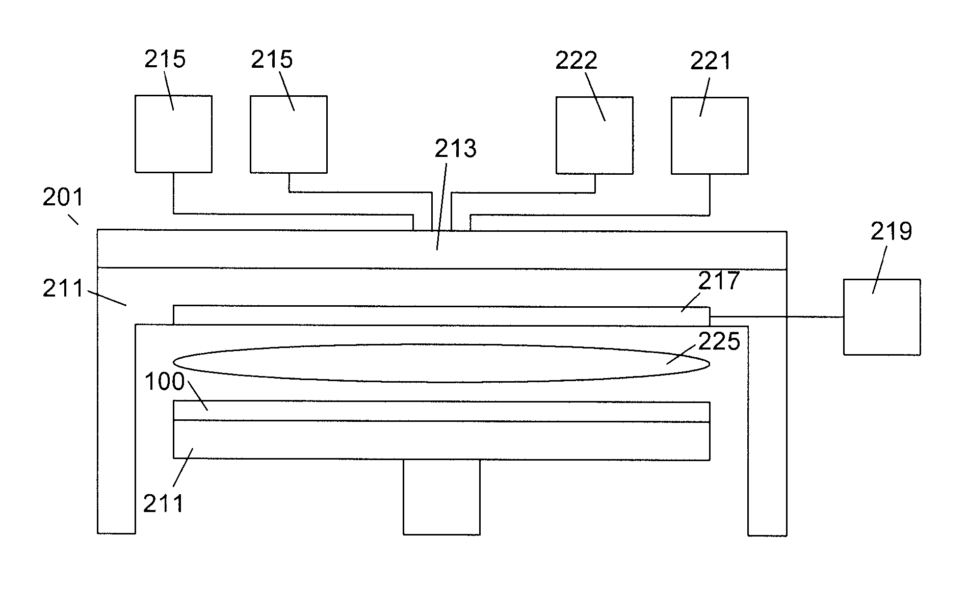
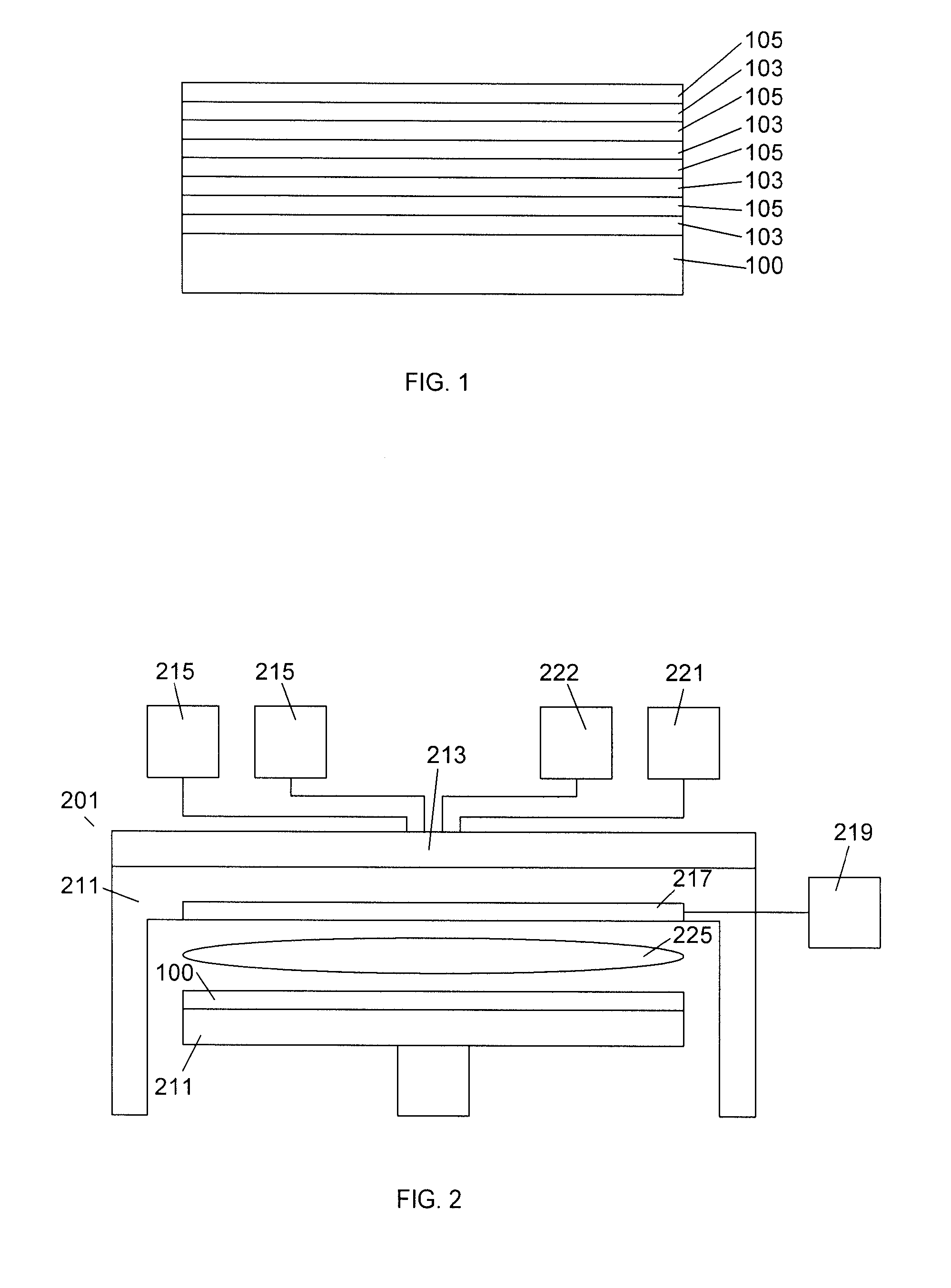
[0023]With reference to FIG. 1, in an embodiment, a multiple layer stack 101 is formed on a substrate 100 having a layer of a first material 103 and a layer of a second material 105. The subsequent layers can repeat this alternating pattern of first material 103 layers and the second material 105. In one embodiment, the first material can be an oxide and the second material can be a nitride. In other embodiments, the first / second material stacks can be oxide / silicon, silicon / doped silicon, or silicon / nitride. All of these combinations of materials can be used in Bit-Cost Scalable (BiCS), Terabit Cell Arry Transistor (TCAT) and other 3D memory structures. In other embodiments, the first / second material stacks can be other combinations of materials. The deposition order of the first and second material layers on the substrate can also be reversed.

[0024]The number of layers can depend upon the memory device being fabricated. In an embodiment, the stack numbers could be 8×, or 16×, or 2...


PUM


Abstract

A layer stack of different materials is deposited on a substrate in a single plasma enhanced chemical vapor deposition processing chamber while maintaining a vacuum. A substrate is placed in the processing chamber and a first processing gas is used to form a first layer of a first material on the substrate. A plasma purge and gas purge are performed before a second processing gas is used to form a second layer of a second material on the substrate. The plasma purge and gas purge are repeated and the additional layers of first and second materials are deposited on the layer stack.

Description

FIELD OF INVENTION[0001]The present invention relates to semiconductor substrate processing systems and, more particularly, to a process for depositing layered stacks of materials.DESCRIPTION OF THE RELATED ART[0002]Semiconductor substrate processing systems generally contain a process chamber having a pedestal for supporting a semiconductor substrate within the chamber proximate a processing region. The chamber forms a vacuum enclosure defining, in part, the process region. A gas distribution assembly or showerhead provides one or more process gases to the process region. The gases are then heated and / or supplied with energy to form a plasma which performs certain processes upon the substrate. These processes may include plasma enhanced chemical vapor deposition (PECVD) to deposit a film upon the substrate.[0003]3D memory can be fabricated from a layer stack of alternating film materials that are deposited on a substrate. For example, the 3D memory can include alternating layers of...

Claims


Application Information

Patent Timeline
IPC IPC(8): H01L21/31
CPCH01L21/02164H01L21/0217H01L21/022H01L21/02274H01L21/0234H01L21/205
Inventor RAJAGOPALAN, NAGARAJANHAN, XINHAIPARK, JI AEKIYOHARA, TSUTOMUPARK, SOHYUNKIM, BOK HOEN
Owner APPLIED MATERIALS INC
Why Eureka
Try Eureka