Method of manufacturing semiconductor device, method of processing substrate and substrate processing apparatus

a technology of semiconductor devices and processing equipment, which is applied in the direction of coatings, coatings, chemical vapor deposition coatings, etc., can solve the problems of difficult to guarantee the thickness uniformity of insulating films, less available sources, and high cost of semiconductor devices, and achieve low cost and high growth rate

Active Publication Date: 2011-12-13
KOKUSA ELECTRIC CO LTD
View PDF5 Cites 354 Cited by
  • Summary
  • Abstract
  • Description
  • Claims
  • Application Information

AI Technical Summary

Benefits of technology

[0009]An object of the present invention is to provide a method of manufacturing a semiconductor device and a substrate processing apparatus wherein an insulating film can be formed at a high growth rate even at a low temperature and the thickness of the insulating film can be uniformly maintained with low costs.

Problems solved by technology

However, since such sources are less available and expensive as compared with conventional source materials, if semiconductor devices are formed by using such sources, the prices of the semiconductor devices may be increased.
In addition, if such sources are used, it is difficult to guarantee the thickness uniformity of an insulating film.

Method used


Image

  • Method of manufacturing semiconductor device, method of processing substrate and substrate processing apparatus
  • Method of manufacturing semiconductor device, method of processing substrate and substrate processing apparatus
  • Method of manufacturing semiconductor device, method of processing substrate and substrate processing apparatus

Examples


examples

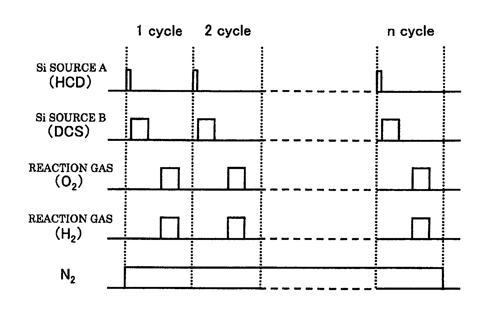
[0148]Silicon oxide films were formed on wafers according to the film-forming sequence of the embodiment of FIG. 4, and film growth rates (SiO film growth rates) and film thickness uniformities in surfaces of the wafers (SiO film thickness uniformities) were measured. Except for the flow rates of HCD and DCS, film-forming conditions (process conditions in each step) were set in the process condition ranges described in the previous embodiments. The flow rate of DCS was kept at a value in the range from 1 slm to 2 slm, the flow rate of HCD was varied in the range from 0 slm to 0.2 slm, and the flow rate ratio of HCD / DCS was varied among (A) 0%, (B) 3%, (C) 6%, and (D) 10%. Hereinafter, these will be referred to as a flow rate condition (A), a flow rate condition (B), a flow rate condition (C), and a flow rate condition (D). The HCD / DCS flow rate ratio at the flow rate condition (A) 0% means the case where HCD was not added to DCS (the case where only DCS was supplied). Furthermore, i...


PUM

PropertyMeasurementUnit
temperatureaaaaaaaaaa
timeaaaaaaaaaa
pressureaaaaaaaaaa

Abstract

Provided is a method of manufacturing a semiconductor device. The method includes: loading a substrate into a process vessel; performing a process to form an oxide, nitride, or oxynitride film on the substrate by alternately repeating: (a) forming a layer containing an element on the substrate by supplying and exhausting first and second source gases containing the element into and from the process vessel; and (b) changing the layer containing the element into an oxide, nitride, or oxynitride layer by supplying and exhausting reaction gas different from the first and second source gases into and from the process vessel; and unloading the substrate from the process vessel. The first source gas is more reactive than the second source gas, and an amount of the first source gas supplied into the process vessel is set to be less than that of the second source gas supplied into the process vessel.

Description

CROSS-REFERENCE TO RELATED PATENT APPLICATION[0001]This U.S. non-provisional patent application claims priority under 35 U.S.C. §119 of Japanese Patent Application Nos. 2009-226420, filed on Sep. 30, 2009, and 2010-152031, filed on Jul. 2, 2010, in the Japanese Patent Office, the entire contents of which are hereby incorporated by reference.BACKGROUND OF THE INVENTION[0002]1. Field of the Invention[0003]The present invention relates to a method of manufacturing a semiconductor device, a method of processing a substrate and a substrate processing apparatus.[0004]2. Description of the Related Art[0005]A flash memory includes an electron accumulation region (floating gate) surrounded by an insulating film and operates in a manner such that information is written in the flash memory by exchanging electrons through a thin tunnel oxide film and the stored information is retained for a long time by holding electrons using the insulating capacity of the thin tunnel oxide layer. Such a flash...

Claims


Application Information

Patent Timeline
Patent Type & Authority Patents(United States)
IPC IPC(8): H01L21/31
CPCH01L21/02189H01L21/02164H01L21/31608H01L21/3145C23C16/45578H01L21/0228C23C16/45546H01L21/3185C23C16/34H01L21/0217C23C16/32C23C16/401H01L21/0214H01L21/02181H01L21/3141H01L21/02178C23C16/45527
Inventor AKAE, NAONORIHIROSE, YOSHIROTAKASAWA, YUSHINOTA, YOSUKESASAJIMA, RYOTA
Owner KOKUSA ELECTRIC CO LTD
Why Eureka
Try Eureka