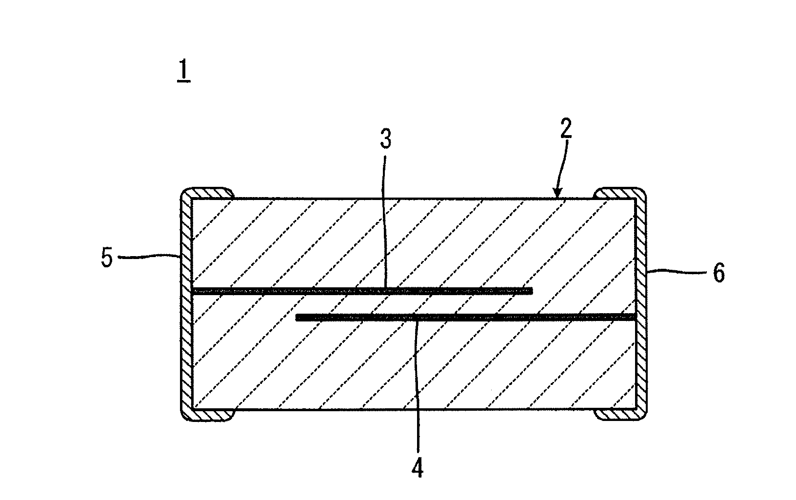
Resistance memory element
a technology of resistor and resistance, applied in the direction of fixed capacitor dielectric, fixed capacitor details, fixed capacitors, etc., can solve the problems of disadvantageously reducing the variation of resistances switched, power consumption increase due to additional resistors, and element cannot be used as a switching element with a relatively high driving voltage, etc., to achieve large resistance variation and high switching characteristics
- Summary
- Abstract
- Description
- Claims
- Application Information
AI Technical Summary
Benefits of technology
Problems solved by technology
Method used
Image

Examples
experimental example 1
[0058]Powdered starting materials were prepared for a semiconductor ceramic of the elementary body, including strontium carbonate (SrCO3), barium carbonate (BaCO3), calcium carbonate (CaCO3) and titanium oxide (TiO2), and donors: lanthanum oxide (La2O3), samarium oxide (Sm2O3), gadolinium oxide (Gd2O3), dysprosium oxide (Dy2O3), yttrium oxide (Y2O3), niobium oxide (Nb2O5) and tantalum oxide (Ta2O5). These starting materials were weighed so that the compositions shown in Tables 1 to 6 were produced after firing.
[0059]Each sample shown in Table 1 contains Ba or Ca as M of the formula {(Sr1-xMx)1-yAy}(Ti1-zBz)O3 and La as A, not containing B (z=0), and the content y of donor A, that is, La, and the amount x of substituent M at the Sr site were varied.
[0060]Each sample shown in Table 2 contains Ba or Ca as M of the formula {(Sr1-xMx)1-yAy}(Ti1-zBz)O3 and Nb as B, not containing A (y=0), and the content z of donor B, that is, Nb, and the amount x of substituent M at the Sr site were vari...
experimental example 2
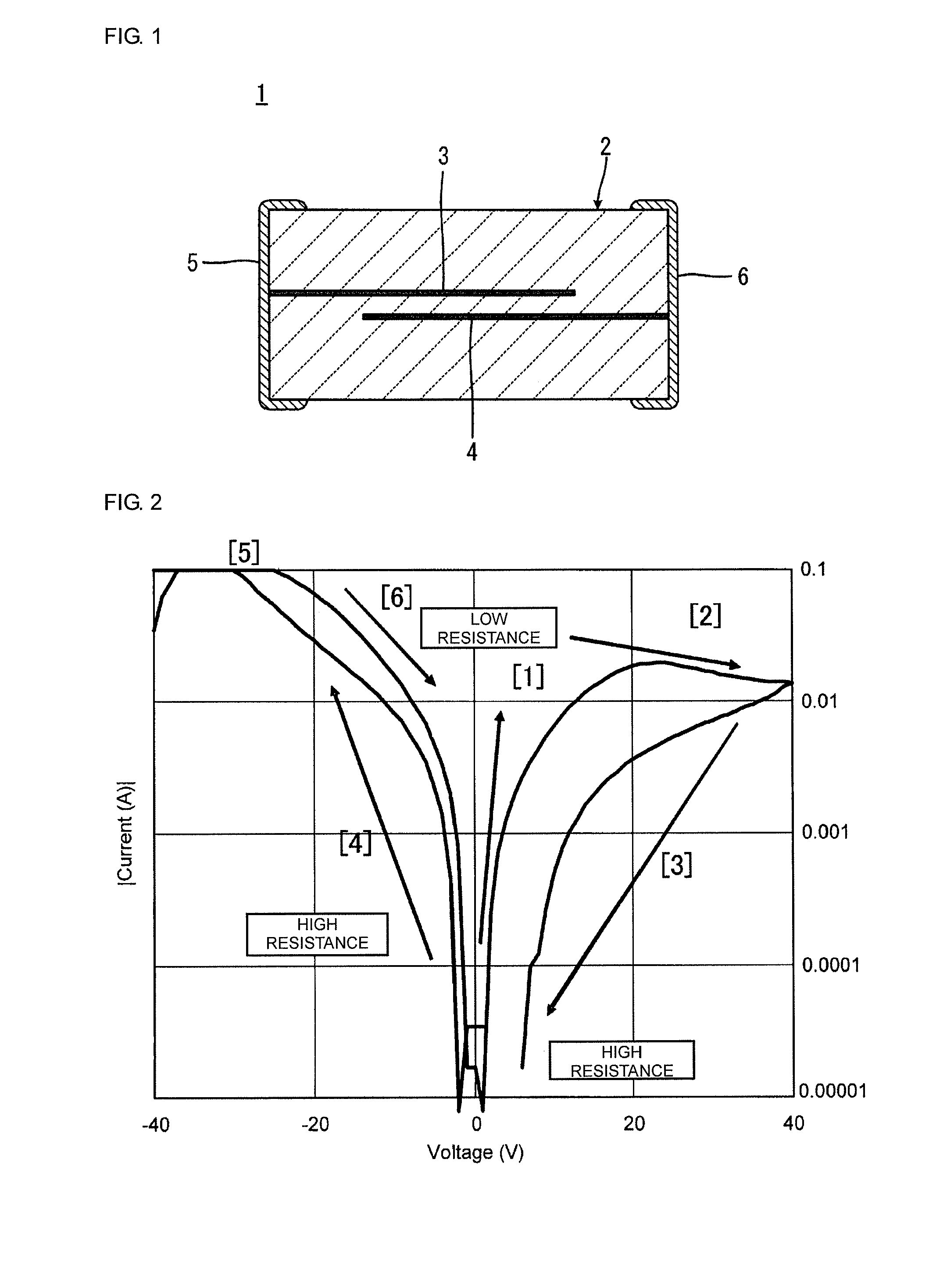
[0083]Samples shown in Tales 7 and 8 were extracted from the samples shown in Tables 1 to 6, and the absolute value of the switching voltage was measured on each sample. The switching voltage mentioned here is defined as the voltage at the inflection point at which the current starts decreasing even though the applied voltage is increased from 0 V, that is, at the point corresponding to +20 V in FIG. 2, in the polarity in which the resistance state in the I-V characteristics is switched from a low resistance state to a high resistance state.
[0084]
TABLE 7{(Sr1−xMx)1−yAy}(Ti1−zBz)O3ResistanceSwitching voltageMABxyzvariation (%)(V)BaLa—0.20.00802500049BaLa—0.40.00802150045BaLa—0.50.00801060040BaLa—0.80.0080750032BaLa—10.0080510022Ba——0.500——BaLa—0.50.00050290068BaLa—0.50.0010530055BaLa—0.50.0030715056BaLa—0.50.00501000045BaLa—0.50.00801060040BaLa—0.50.0101100040BaLa—0.50.020560042BaLa—0.50.030220051Ba——0.500——Ba—Nb0.500.0005250071Ba—Nb0.500.001520056Ba—Nb0.500.003730060Ba—Nb0.500.00513...
PUM
| Property | Measurement | Unit |
|---|---|---|
| switching voltage | aaaaa | aaaaa |
| switching voltage | aaaaa | aaaaa |
| rated voltage | aaaaa | aaaaa |
Abstract
Description
Claims
Application Information
 - R&D
- Intellectual Property
- Life Sciences
- Materials
- Tech Scout
- Unparalleled Data Quality
- Higher Quality Content
- 60% Fewer Hallucinations
Browse by: Latest US Patents, China's latest patents, Technical Efficacy Thesaurus, Application Domain, Technology Topic, Popular Technical Reports.
© 2025 PatSnap. All rights reserved.Legal|Privacy policy|Modern Slavery Act Transparency Statement|Sitemap|About US| Contact US: help@patsnap.com