Method for manufacturing diamond monocrystal having a thin film, and diamond monocrystal having a thin film

a technology of monocrystal and diamond monocrystal, which is applied in the field of diamond monocrystal having a thin film, can solve the problems of large fluctuation of the specific resistance of the thin film and the angle or surface roughness thereof, and achieves the effects of low resistance, minimal fluctuation and low cos

Active Publication Date: 2012-02-21
SUMITOMO ELECTRIC IND LTD
View PDF13 Cites 4 Cited by
  • Summary
  • Abstract
  • Description
  • Claims
  • Application Information

AI Technical Summary

Benefits of technology

[0014]The diamond monocrystal having a low-resistance phosphorus-doped diamond epitaxial thin film, and the method for manufacturing a diamond monocrystal having a low-resistance phosphorus-doped diamond epitaxial thin film according to the present invention make it possible to provide a diamond monocrystal having a low-resistance phosphorus-doped diamond epitaxial thin film, and a method for manufacturing a diamond monocrystal having a low-resistance phosphorus-doped diamond epitaxial thin film having minimal fluctuation of specific resistance, through the use of a {111} monocrystal substrate having prescribed off-angle, and the application of a prescribed range of vapor-phase synthesis conditions.
[0015]The diamond monocrystal having a low-resistance phosphorus-doped diamond epitaxial thin film according to the present invention has low resistance and minimal fluctuation of specific resistance, and can therefore be applied as a material used in environment-resistant devices that operate in high-temperature environments or space environments, power devices capable of high-frequency and high-output operation, luminescent devices capable of emitting ultraviolet light, electron emission devices capable of low-voltage operation, or other semiconductor devices / electronic devices.

Problems solved by technology

However, the angle or surface roughness thereof fluctuates due to the difficulty of grinding.
As a result, problems occur in that the specific resistance of the thin films and the phosphorus concentration in the thin films fluctuate widely between test samples.

Method used


Image

  • Method for manufacturing diamond monocrystal having a thin film, and diamond monocrystal having a thin film
  • Method for manufacturing diamond monocrystal having a thin film, and diamond monocrystal having a thin film
  • Method for manufacturing diamond monocrystal having a thin film, and diamond monocrystal having a thin film

Examples


example 1

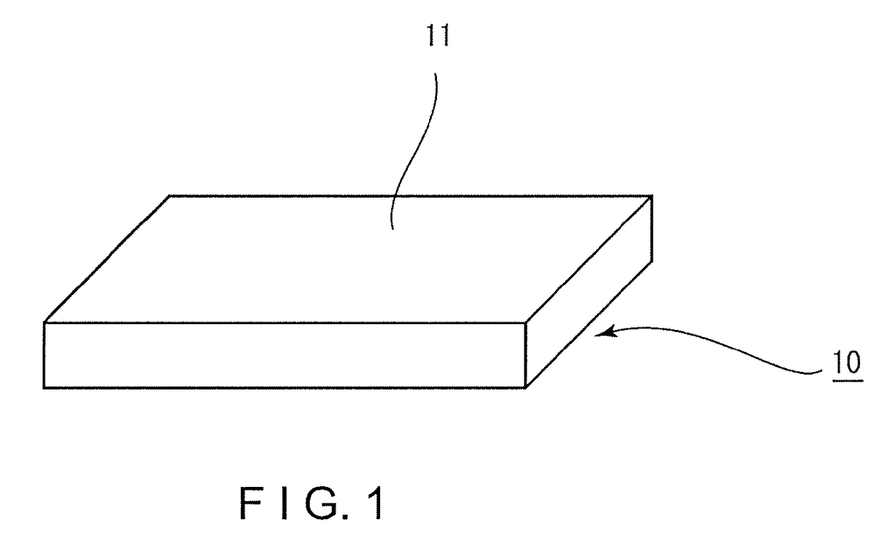
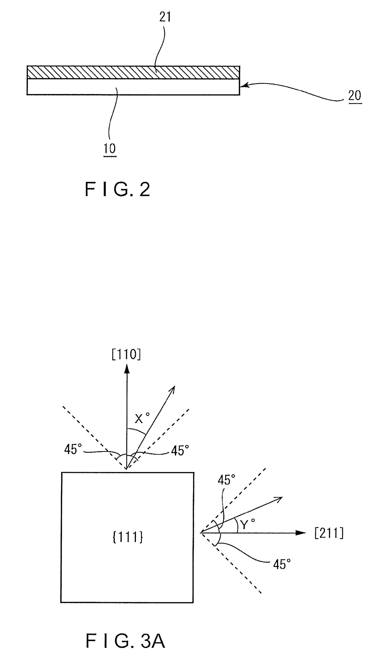
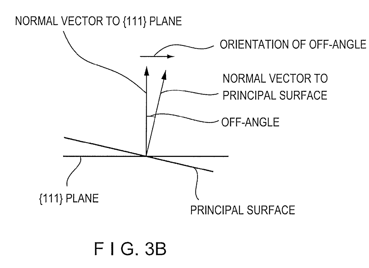
[0043]A plurality of IIa-type diamond {111} monocrystal substrates 10 such as the one shown in FIG. 1 synthesized at high temperature and high pressure was prepared, and each had a surface roughness of 10 nm, a size of 2.0 mm×2.0 mm×0.3 mm thick, an off-angle of the principal surface 11 controlled to 0.49° to 3.29°, and a tilt orientation of the normal vector to the principal surface 11 controlled to 40° with respect to the [110] direction. Phosphorus-doped diamond epitaxial thin films were synthesized on the principal surfaces 11 by a microwave plasma CVD device. Hydrogen, methane, and phosphine were used as source gases, and the synthesis conditions were a methane gas flow rate / hydrogen gas flow rate ratio of 0.05%, a phosphine gas flow rate / methane gas flow rate ratio (PH3 / CH4, vapor-phase phosphorus atom [P] / carbon atom [C] ratio) of 3 to 20%, a gas-mixture pressure of 1.3×10⁴ Pa, a substrate temperature of 870° C., and a synthesis time of 5 hours.

[0044]The synthesized thin film...

example 2

[0047]A plurality of IIa-type diamond {111} monocrystal substrates 10 such as the one shown in FIG. 1 synthesized at high temperature and high pressure was prepared, and each had a surface roughness of 10 nm, a size of 2.0 mm×2.0 mm×0.3 mm thick, an off-angle of the principal surface 11 controlled to 0.51° to 3.16°, and a tilt orientation of the normal vector to the principal surface 11 controlled to 1.7° to 43.3° with respect to the [110] direction. Phosphorus-doped diamond epitaxial thin films were synthesized on the principal surfaces 11 by a microwave plasma CVD device. Hydrogen, methane, and phosphine were used as source gases, and the synthesis conditions were a methane gas flow rate / hydrogen gas flow rate ratio of 0.05%, a phosphine gas flow rate / methane gas flow rate ratio (PH3 / CH4, vapor-phase phosphorus atom [P] / carbon atom [C] ratio) of 3 and 10%, a gas-mixture pressure of 1.3×10⁴ Pa, a substrate temperature of 870° C., and a synthesis time of 5 hours. Evaluation of the s...

example 3

[0050]A plurality of IIa-type diamond {111} monocrystal substrates 10 such as the one shown in FIG. 1 synthesized at high temperature and high pressure was prepared, and each had a surface roughness of 10 nm, a size of 2.0 mm×2.0 mm×0.3 mm thick, an off-angle of the principal surface 11 controlled to 0.51° to 3.16°, and a tilt orientation of the normal vector to the principal surface 11 controlled to 1.7° to 43.3° with respect to the [211] direction. Phosphorus-doped diamond epitaxial thin films were synthesized on the principal surfaces 11 by a microwave plasma CVD device. Hydrogen, methane, and phosphine were used as source gases, and the synthesis conditions were a methane gas flow rate / hydrogen gas flow rate ratio of 0.05%, a phosphine gas flow rate / methane gas flow rate ratio (PH3 / CH4, vapor-phase phosphorus atom [P] / carbon atom [C] ratio) of 3 and 10%, a gas-mixture pressure of 1.3×10⁴ Pa, a substrate temperature of 870° C., and a synthesis time of 5 hours. The synthesized thi...


PUM

PropertyMeasurementUnit
off-angleaaaaaaaaaa
surface roughnessaaaaaaaaaa
carrier mobilityaaaaaaaaaa

Abstract

A method for growing a low-resistance phosphorus-doped epitaxial thin film having a specific resistance of 300 Ωcm or less at 300 K on a principal surface of a {111} monocrystal substrate under conditions in which the phosphorus atom / carbon atom ratio is 3% or higher, includes the principal surface having an off-angle of 0.50° or greater. The diamond monocrystal having a low-resistance phosphorus-doped diamond epitaxial thin film is such that the thin-film surface has an off-angle of 0.50° or greater with respect to the {111} plane, and the specific resistance of the low-resistance phosphorus-doped diamond epitaxial thin film is 300 Ωcm or less at 300 K.

Description

TECHNICAL FIELD[0001]The present invention relates to a method for manufacturing a diamond monocrystal having a phosphorus-doped diamond epitaxial thin film, and to a diamond monocrystal having a phosphorus-doped diamond epitaxial thin film.BACKGROUND ART[0002]Diamond as a semiconductor material has an extremely large band gap of 5.5 eV, and a high carrier mobility of 2000 cm2 / V·s at room temperature for both electrons and positive holes. The dielectric constant is also small, being 5.7, and the breakdown field is high, being 5×10⁶ V / cm. Furthermore, diamond also has the rare characteristic of negative electron affinity in which the vacuum level exists below the lower end of the conduction band. Because of such excellent characteristics, diamond has potential applications as a material for semiconductor devices such as environment-resistant devices that operate in high-temperature environments or space environments, power devices capable of high-frequency and high-output operation, ...

Claims


Application Information

Patent Timeline
Patent Type & Authority Patents(United States)
IPC IPC(8): C30B29/04
CPCC30B25/02C30B25/105C30B29/04H01L21/02376H01L21/02433H01L21/02576H01L21/02609H01L21/0262H01L21/02527Y10T428/30Y10T428/24355
Inventor UEDA, AKIHIKOMEGURO, KIICHIYAMAMOTO, YOSHIYUKINISHIBAYASHI, YOSHIKIIMAI, TAKAHIRO
Owner SUMITOMO ELECTRIC IND LTD
Why Eureka
Try Eureka