Inspection system and method for high-speed serial data transfer

a data transfer and serial technology, applied in the field of serial data transfer inspection systems, can solve problems such as device failure, data transfer methods, and conventional inspection systems that fail to maximize inspection speed, reliability and scalability,

Active Publication Date: 2012-03-20
KLA TENCOR TECH CORP
View PDF31 Cites 11 Cited by
  • Summary
  • Abstract
  • Description
  • Claims
  • Application Information

AI Technical Summary

Benefits of technology

[0024]The optical transceiver is coupled to the programmable element for converting each encoded data packet into an optical signal, which is transferred serially over a single fibre channel. In most embodiments, the fibre channel p

Problems solved by technology

For instance, detecting defects of decreasing size has become increasingly necessary, since even relatively small defects may cause unwanted aberrations in the semiconductor device, sometimes causing the device to fail.
Regardless of the processing configuration used, conventional inspection systems typically fail to maximize inspection speed, reliability and scalability.
Such data transfer methods suffer from limited data transfer rates, signal integrity problems and require numerous wires and connectors, which are bulky and unreliable.
As set forth below, internal processing

Method used


Image

  • Inspection system and method for high-speed serial data transfer
  • Inspection system and method for high-speed serial data transfer
  • Inspection system and method for high-speed serial data transfer

Examples


Embodiment Construction

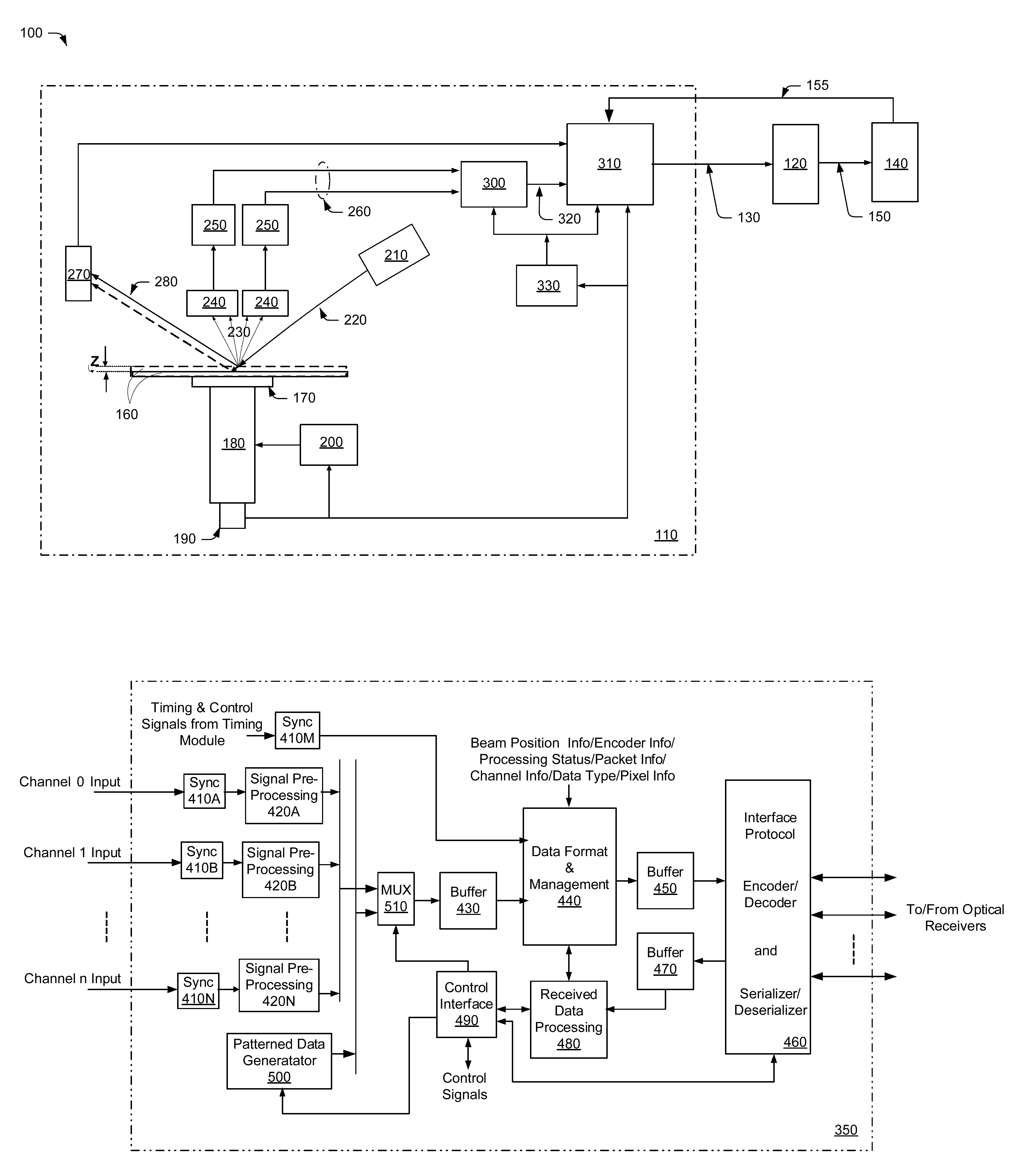
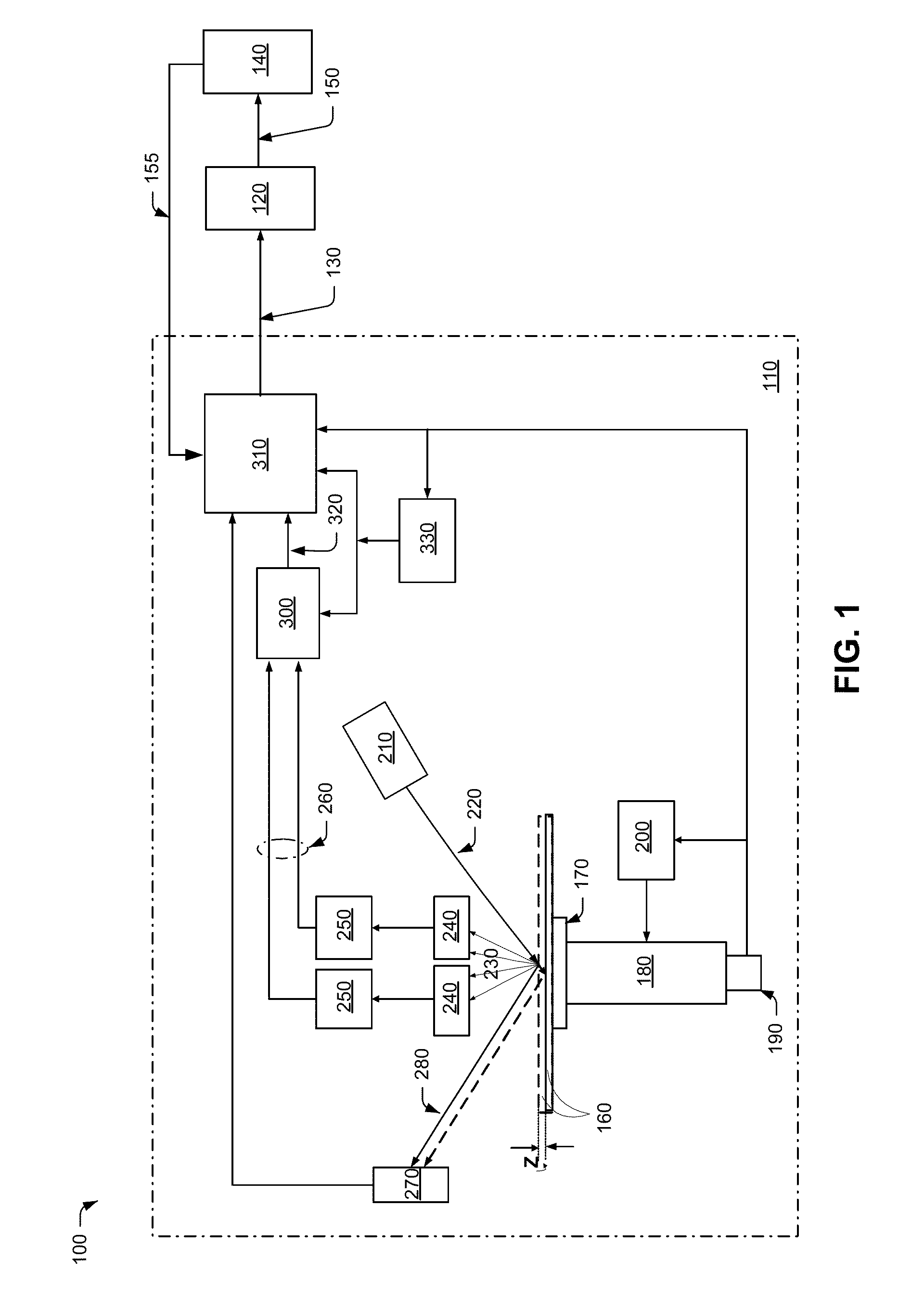
[0038]As used herein, the term “specimen” refers to a reticle or a wafer. The terms “reticle” and “mask” are used interchangeably herein. A reticle generally includes a transparent substrate such as glass, borosilicate glass, and fused silica having opaque regions formed thereon in a pattern. In some cases, the opaque regions may be replaced by regions etched into the transparent substrate. In some cases, the pattern may be replicated one or more times, such that a plurality of “dice” are formed on the substrate. Many different types of reticles are known in the art, and the term reticle as used herein is intended to encompass all types of reticles.

[0039]As used herein, the term “wafer” generally refers to substrates formed of a semiconductor or non-semiconductor material. Examples of a semiconductor or non-semiconductor material include, but are not limited to, monocrystalline silicon, gallium arsenide, and indium phosphide. Such substrates may be commonly found and / or processed in...


PUM


Abstract

An inspection system and method for serial high-speed image data transfer is provided herein. According to one embodiment, the method may include receiving multiple channels of image data at an input data rate and buffering the image data at the input data rate until the buffered data reaches a predetermined size. Once the predetermined size has been reached, the method may include packing the buffered data, encoding the data packet, serializing the encoded data packet and converting the encoded data packet into an optical signal. In some cases, the image data may be packed along with a data header containing information about the system. Once converted, each optical signal (i.e., representing one data packet) may be transmitted serially over one or more fibre channels to a processing node of the inspection system. In most cases, the data is packed, encoded, serialized and transmitted to the processing node at a data rate much higher than the input data rate. The processing node analyzes the optical signal to detect defects on a specimen under inspection.

Description

BACKGROUND OF THE INVENTION[0001]1. Field of the Invention[0002]This invention relates to semiconductor inspection and, more particularly, to inspection systems and methods for transferring and processing inspection images.[0003]2. Description of the Related Art[0004]The following descriptions and examples are given as background only.[0005]Semiconductor devices, such as logic, memory and other integrated circuit devices, are fabricated by processing a specimen (such as a semiconductor wafer) to form various features and multiple levels of the semiconductor device. Lithography is one example of a semiconductor fabrication process that may be used to transfer a pattern to a resist arranged on a semiconductor wafer. Additional examples of semiconductor fabrication processes include, but are not limited to, chemical-mechanical polishing, etch, deposition, and ion implantation. Multiple semiconductor devices can be fabricated in an arrangement on a semiconductor wafer and then separated...

Claims


Application Information

Patent Timeline
IPC IPC(8): G06K9/00
CPCG01N21/8851G01N21/9501G01N2021/8825G01N2021/8864G01N2021/8896G01N2021/95676G01N2201/1045
Inventor CHU, YUNXIANSLOBODOV, ALEXANDER
Owner KLA TENCOR TECH CORP
Why Eureka
Try Eureka