High frequency switch circuit comprising a transistor on the high frequency path

a high-frequency switch and path technology, applied in the direction of electronic switching, basic electric elements, pulse techniques, etc., can solve the problems of reduced withstand power characteristics, increased on-resistance of field-effect transistors, circuits that cannot function as switches, etc., and achieve the effect of easy integration

Active Publication Date: 2012-04-17
HITACHI METALS LTD
View PDF21 Cites 20 Cited by
  • Summary
  • Abstract
  • Description
  • Claims
  • Application Information

AI Technical Summary

Benefits of technology

[0030]According to the present invention, it is possible to directly control a high frequency switch circuit by a logic circuit using a low voltage as its operating voltage. This contributes to reduce the voltage of logic circuits in a wireless communication terminal, and to thereby reduce power consumption of the wireless communication terminal.
[0031]Further, this circuit can be integrated by semiconductor process for depletion type pHEMT (Pseudomorphic High Electron-Mobility Transistor) which has already been put in practical use, and hence can be produced at a low cost.
[0032]Further, since the gate of the above described depletion type field-effect transistor is grounded via the resistor, even when an excessive voltage is applied to the external-control-signal-input terminal, it is possible to prevent the thermal destruction of the field-effect transistor by suppressing the current, and to thereby contribute to the improvement in reliability of the high frequency switch circuit.
[0033]Further, the high frequency switch circuit is constituted by using only the depletion type field-effect transistors having substantially the same pinch-off voltage as an active element, which makes it possible to realize the circuit without adding a new process in the case of integration, at a low cost. Alternatively, by substituting an active load for the resistor in the control-voltage-generating circuit, it is also possible to save the chip area in the case of integrating the circuit and to thereby reduce the cost.
[0034]Alternatively, in the present invention, by connecting the internal-control-voltage-output terminal to the switch circuit via the low pass filter consisting of the resistor and the capacitor, it is possible to realize means for preventing the generation of harmonics and instability due to the feedback of a signal, without obstructing the integration, and easily.

Problems solved by technology

However, in the high frequency switch circuit disclosed in Patent Document 1, when the change in the control voltage is not sufficiently large as compared with the absolute value of pinch-off voltage of the depletion type field-effect transistor used in the circuit, the circuit becomes unable to function as the switch.
This results in a problem that the withstand power characteristic is reduced.
The above described problem of the withstand power characteristic can be solved by bringing the pinch-off voltage close to 0 V. However, when the pinch-off voltage is brought close to 0 V, the on-resistance of the field-effect transistor is increased, so that the insertion loss of the high frequency switch circuit is increased.
For the above described reason, in the high frequency switch circuit proposed in Patent Document 1, there is a high probability that a problem may arise when an output of a logic circuit whose voltage is lowered is used as it is for the control of the high frequency switch circuit.
Further, in the inverter circuit constitution described in Patent Document 2, there is a disadvantage that even when the output terminal of the inverter is in a Low state, a voltage twice the on-voltage of a diode is output so as to reduce the change in the output voltage.
This results in the same problem, as in the case of Patent Document 1, that the withstand power characteristic is reduced.
This results in a problem that a power source needs to be separately provided for the switch circuit, or that the number of elements constituting the circuit is large.
Further, in Patent Document 4, there is a problem that in the booster circuit of any of the proposed systems (FIG. 11, FIG. 12, FIG. 13, FIG. 14 in Patent Document 4), even in the case where the external control voltage is set to be low, when a high-power high frequency signal is applied to a high-frequency-detection terminal, a potential due to the rectifying action is added so as to increase the output voltage, and thereby a sufficient signal isolation performance cannot be obtained.

Method used


Image

  • High frequency switch circuit comprising a transistor on the high frequency path
  • High frequency switch circuit comprising a transistor on the high frequency path
  • High frequency switch circuit comprising a transistor on the high frequency path

Examples


embodiment 1

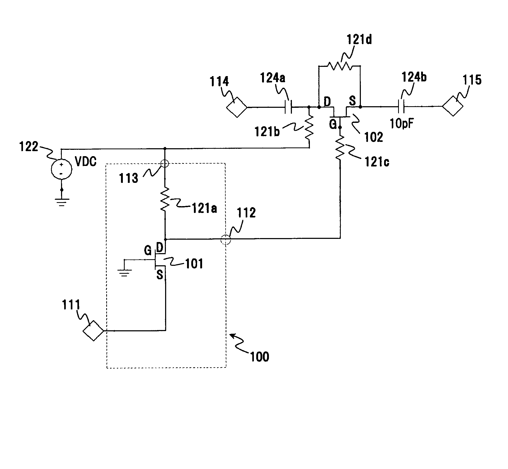
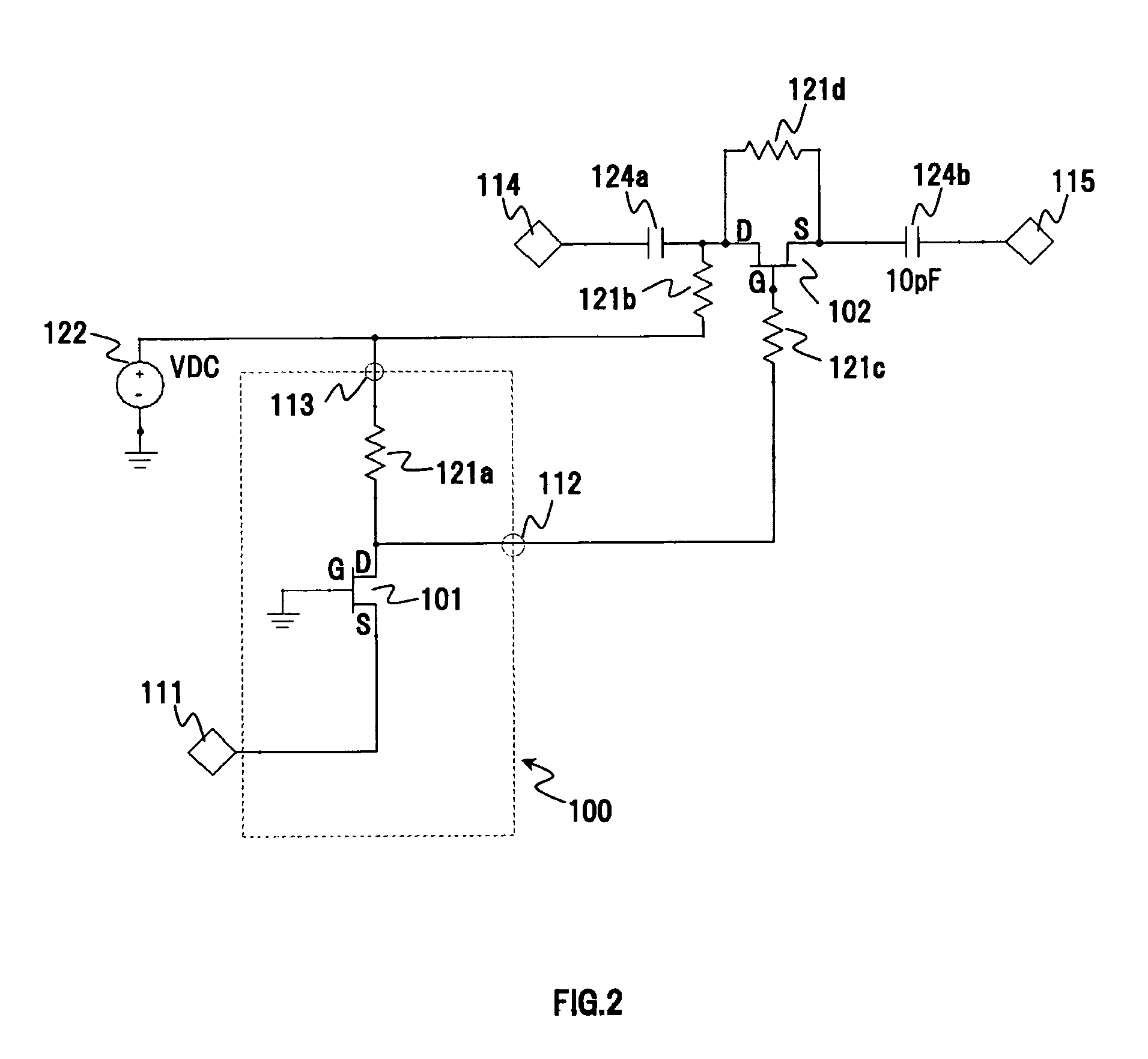
[0049]FIG. 2 is a circuit diagram of a high frequency switch circuit as a first embodiment according to the present invention. In the figure, reference numerals 114 and 115 denote an input terminal 114 and an output terminal 115 of a high frequency signal in the high frequency switch circuit, respectively. Reference numerals 101 and 102 denote depletion type field-effect transistors, and reference characters 121a to 121d denote resistors. The input terminal 114 and output terminal 115 of the high frequency signal are provided via a switch circuit including the depletion type field-effect transistor 102 for performing switching between a connection state and a disconnection state of a high frequency signal path.

[0050]Note that in the present embodiment, the resistor 121a used in a control-voltage-generating circuit 100 is a resistor formed of a tantalum nitride thin film. Further, reference characters 124a and 124b denote capacitors serving as a sufficiently small impedance in a high...

embodiment 2

[0063]FIG. 4 is a circuit diagram of a high frequency switch circuit as a second embodiment according to the present invention. Note that in the figure, the same elements as those shown in FIG. 2 are denoted by the same numerals and characters. In this high frequency switch circuit, the gate of a field-effect transistor 101 used in a control-voltage-generating circuit 100 is grounded via a resistor 121e.

[0064]Since the gate of the field-effect transistor 101 is grounded via the resistor 121e in this way, even when an excessive voltage is input from an external-control-signal-input terminal 111, the current caused by the excessive voltage necessarily flows through a resistor 121a or the resistor 121e, so that the voltage applied to the field-effect transistor 101 (current flowing through the transistor) is suppressed.

[0065]In this way, the field-effect transistor 101 is protected to some extent against an input of overvoltage, and hence it is possible to expect that the reliability ...

embodiment 3

[0069]FIG. 5 is a circuit diagram of a high frequency switch circuit as a third embodiment according to the present invention. In the present embodiment, a single-pole-double-throw (SPDT) circuit is realized. Note that also in FIG. 5, the same elements as those shown in FIG. 2 are denoted by the same reference numerals and characters. However, in correspondence with the high frequency switch circuit being provided with two control-voltage-generating circuits (100a, 100b), suffixes a and b are respectively attached to components of the control-voltage-generating circuits, for example, as in external-control-signal-input terminals 111a and 111b.

[0070]In the following, an operation of the high frequency switch circuit according to the present embodiment will be described. The high frequency switch circuit according to the present embodiment includes the two control-voltage-generating circuits 100a and 100b, and complementary external control signal voltages from a logic circuit are ap...


PUM


Abstract

A high frequency switch circuit according to the present invention includes a control-voltage-generating circuit. The control-voltage-generating circuit includes a depletion type field-effect transistor, an external-control-signal-input terminal, an internal-control-voltage-output terminal, and a power-receiving terminal of the control-voltage-generating circuit. The field-effect transistor has a grounded gate, a source connected to the external-control-signal-input terminal, and a drain connected to the power-receiving terminal. The internal-control-voltage-output terminal is connected to an electrical connection path between the drain of the field-effect transistor and the power-receiving terminal.

Description

TECHNICAL FIELD[0001]The present invention relates to a high frequency switch circuit constituted by using, in particular, a depletion type field-effect transistor, such as a high electron mobility transistor, in a switch circuit for switching a connection path of a high frequency signal.BACKGROUND ART[0002]In a radio communication apparatus for switching transmission and reception in time division, it is necessary to switch the connection between an antenna and a transmission / reception circuit. Alternatively, in a terminal using a plurality of frequency bands, a plurality of transmission / reception circuits are generally incorporated for the respective frequency bands, and hence it is necessary to switch signal paths between an antenna and the transmission / reception circuits. Alternatively, in a radio communication apparatus adopting diversity reception or MIMO (Multi Input Multi Output) systems, it is necessary to switch signal paths between a plurality of antennas and transmission...

Claims


Application Information

Patent Timeline
Patent Type & Authority Patents(United States)
IPC IPC(8): H03K17/687H01P1/32
CPCH03K17/693H03K2017/6875H03K2017/0806H03K17/687
Inventor SUGIYAMA, YUTA
Owner HITACHI METALS LTD
Why Eureka
Try Eureka