

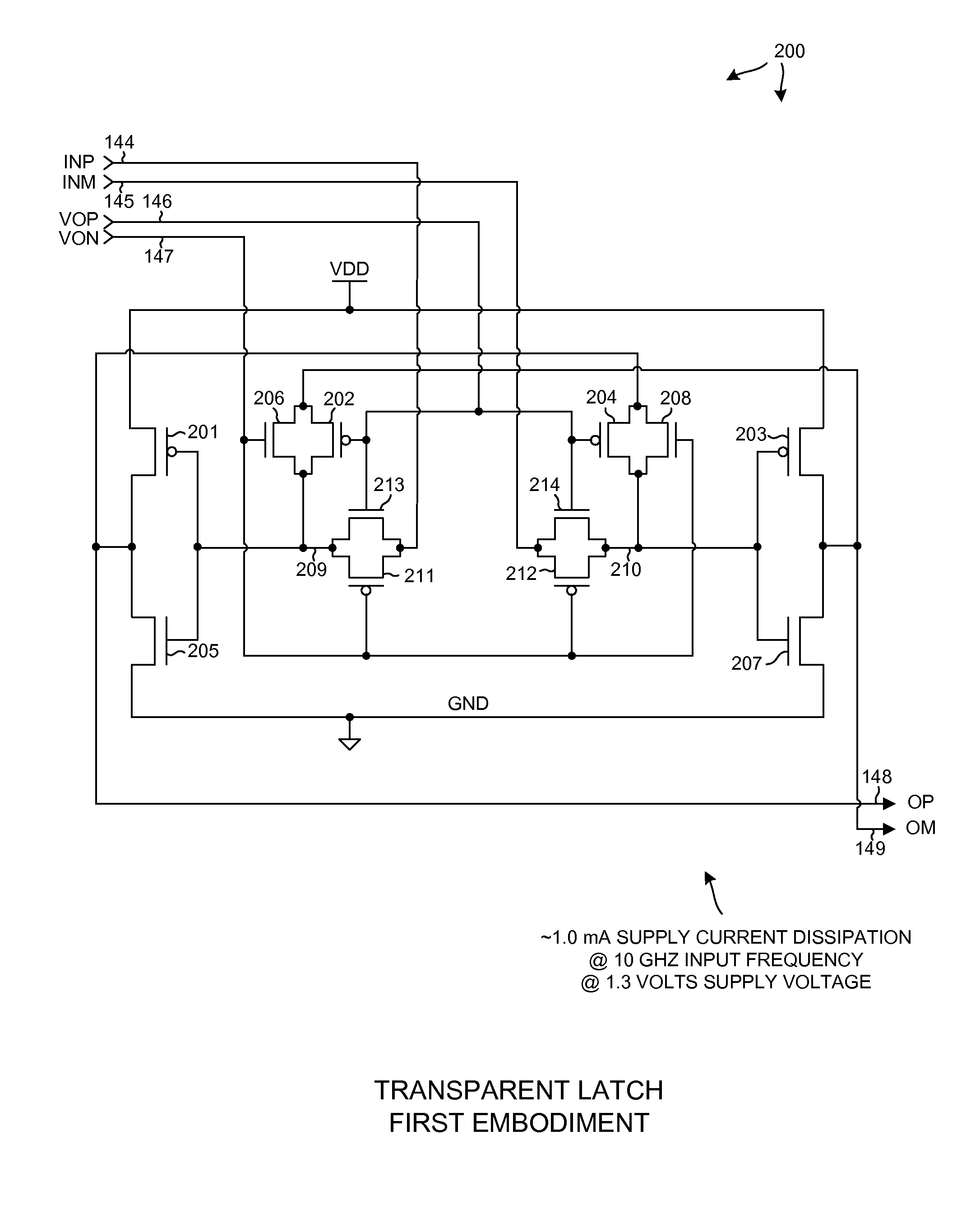
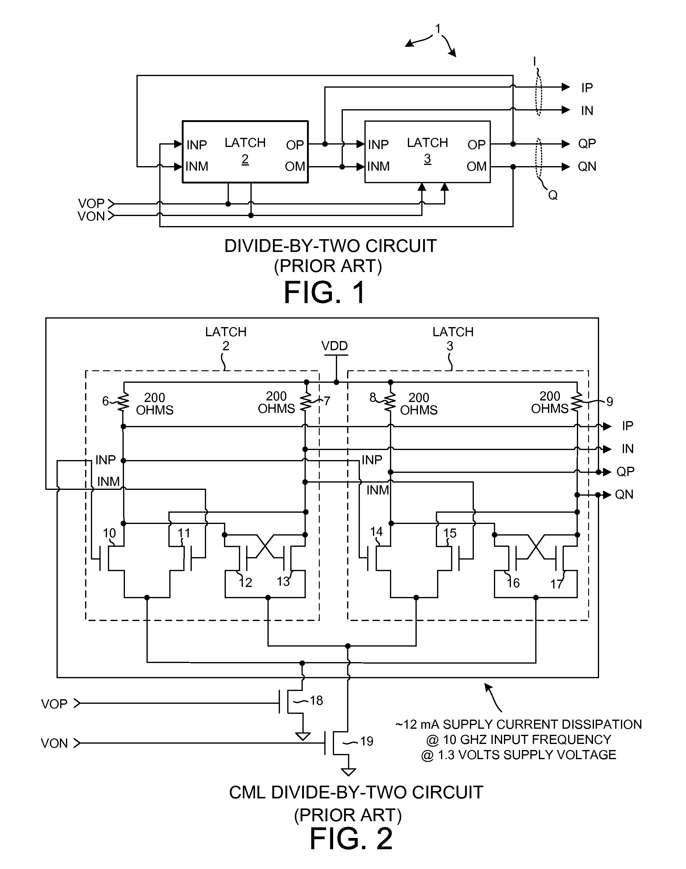
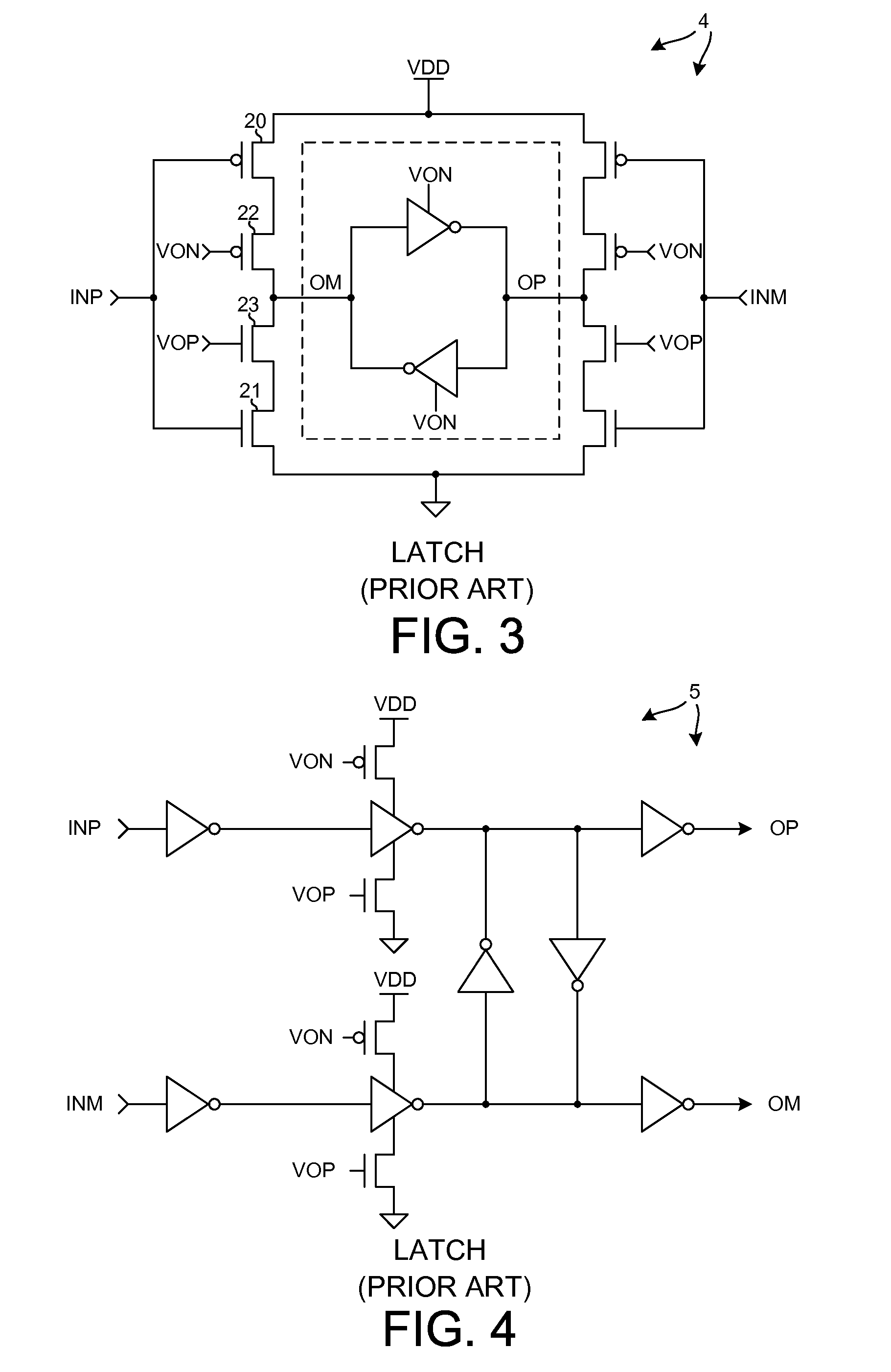
Low power complementary logic latch and RF divider
a low-power, complementary logic technology, applied in the direction of instruments, computation using denominational number representation, pulse technique, etc., can solve the problems of circuits that consume a 12 milliamperes, latches of fig. 4 consume an undetectable large amount of supply current, etc., to improve signal headroom and footroom, improve speed advantage, and low supply voltage
- Summary
- Abstract
- Description
- Claims
- Application Information
AI Technical Summary
Benefits of technology
Problems solved by technology
Method used
Image

Examples
Embodiment Construction
[0033]FIG. 5 is a diagram of an example of a device that includes a novel divider circuit. The device is a mobile communication device 100. The novel divider circuit is, however, a circuit of general applicability and is usable in other radio circuits, including Wireless Local Area Network (WLAN) radio circuits, and other circuits other than radio circuits. Mobile communication device 100 in the example described below is a cellular telephone. Device 100 includes (among other parts not illustrated) an antenna 101 usable for receiving and transmitting cellular telephone communications, an RF transceiver integrated circuit 102, and a digital baseband integrated circuit 103.
[0034]FIG. 6 is a more detailed diagram of the RF transceiver integrated circuit 102 of FIG. 5. In one very simplified explanation of the operation of device 100, if device 100 is being used to receive audio information as part of a cellular telephone conversation, then an incoming transmission 104 is received on an...
PUM
 Abstract
Description
Claims
Application Information