

Metal laminated body, LED-mounted substrate, and white film
a technology of led-mounted substrates and laminated bodies, which is applied in the direction of discharge tubes/lamp details, thermoplastic polymer dielectrics, synthetic resin layered products, etc., can solve the problems of difficult future general lighting and substrate use for display, the limitation of ceramic substrates for larger-size and lower-profile products, etc., and achieve excellent dimensional stability, high reflectance, and high thermal resistance
- Summary
- Abstract
- Description
- Claims
- Application Information
AI Technical Summary
Benefits of technology
Problems solved by technology
Method used
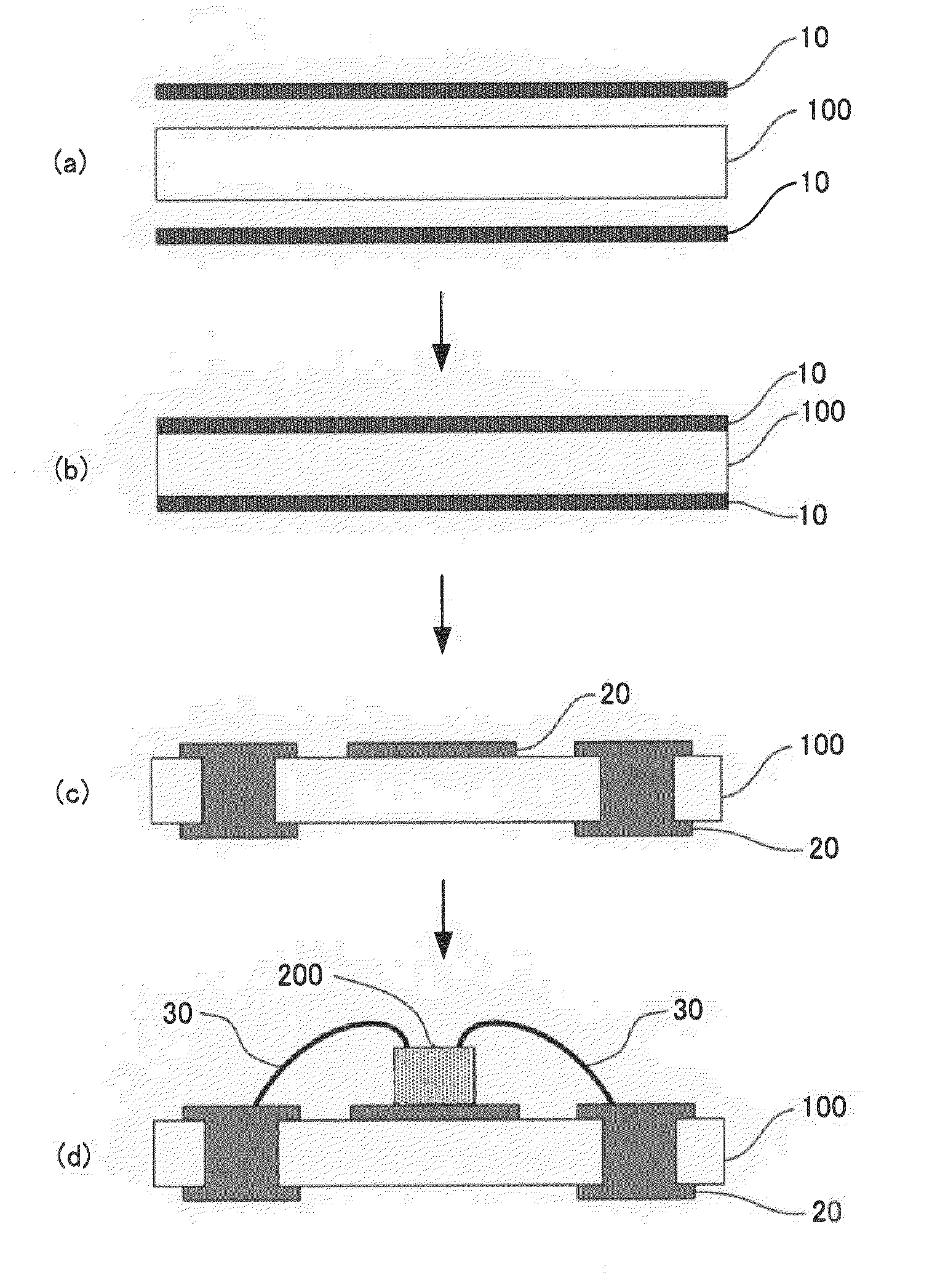
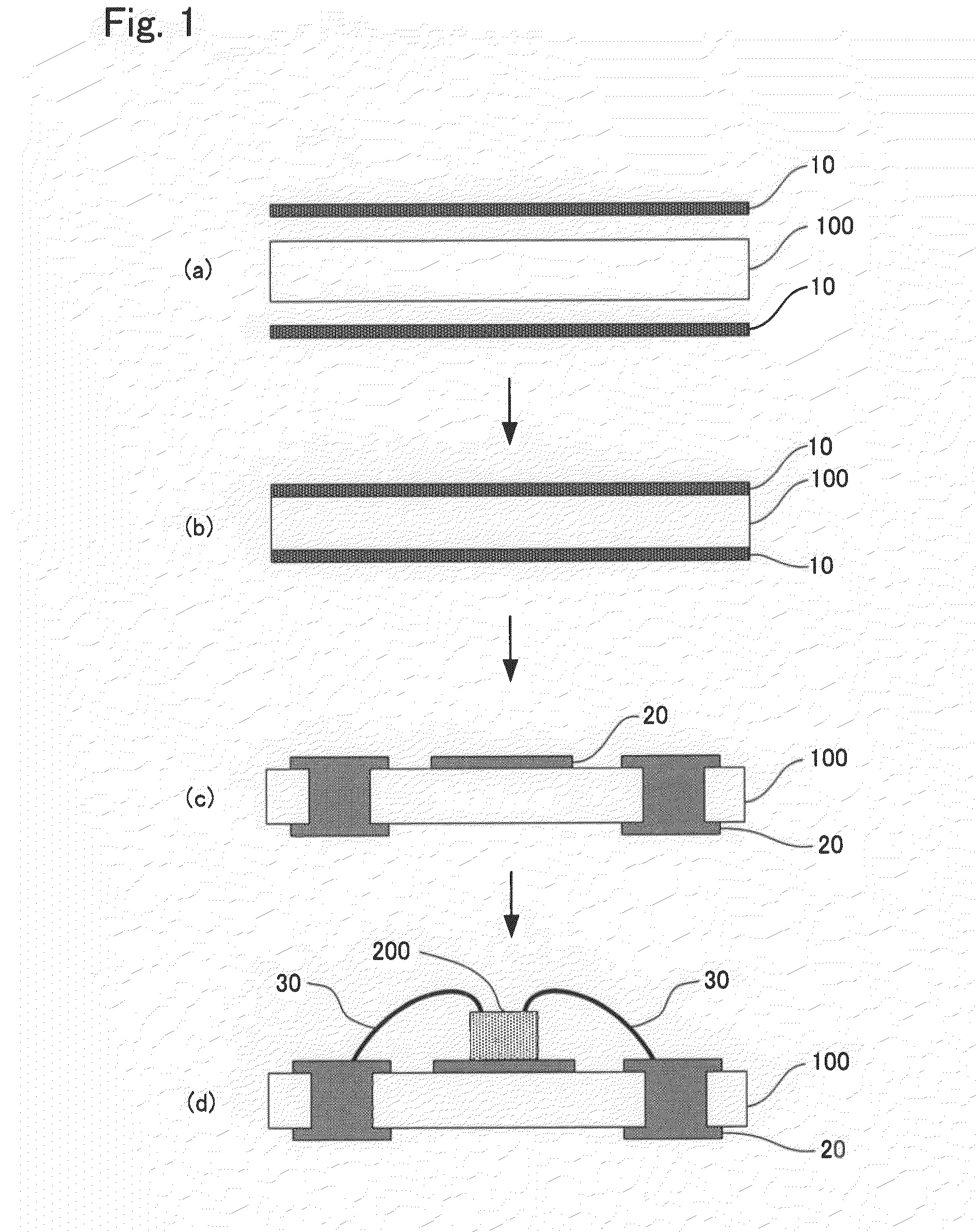
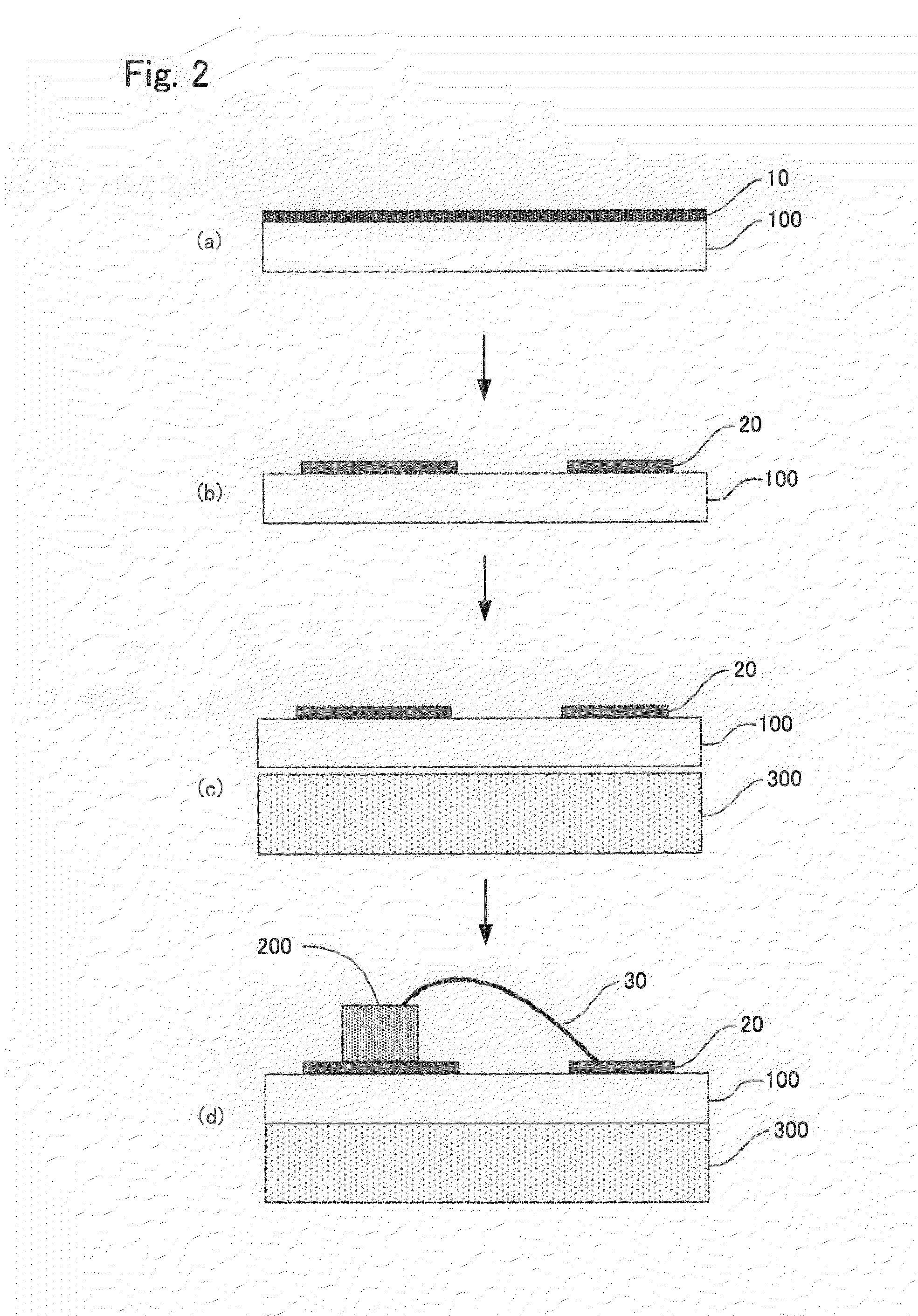
Image

Examples
example 1
[0098]A thermoplastic resin composition obtained by mixing: 100 parts by mass of a resin composition comprising 60 mass % of polyether ether ketone resin (“PEEK 450G”, Tm=335° C.) and 40 mass % of amorphous polyetherimide resin (“ULTEM 1000”); 30 parts by mass of a titanium oxide (average particle diameter: 0.23 μm, treated with alumina and a silane coupling agent) produced by chlorine method; and 21 parts by mass of synthetic mica having an average particle diameter of 5 μm and an average aspect ratio of 50 was melt-kneaded. Then, the melt-kneaded thermoplastic resin composition was formed into a 100 μm thick film using an extruder having T-dies at a set temperature of 380° C. The evaluation results are shown in Table 1.
example 2
[0099]Except for using a resin mixture comprising: 40 mass % of polyether ether ketone resin (“PEEK 450G”, Tm=335° C.); and 60 mass % of amorphous polyetherimide resin (“ULTEM 1000”), Example 2 was carried out in the same manner as Example 1 to produce a 100 μm thick film. The evaluation results are shown in Table 1.
example 3
[0100]Except for using a thermoplastic resin composition obtained by mixing: 35 parts by mass of titanium oxide; and 30 parts by mass of a synthetic mica having an average particle diameter of 5 μm and an average aspect ratio of 50, Example 3 was carried out in the same manner as Example 1 to produce a 100 μm thick film. The evaluation results are shown in Table 1.
PUM
| Property | Measurement | Unit |
|---|---|---|
| reflectance | aaaaa | aaaaa |
| reflectance | aaaaa | aaaaa |
| average particle diameter | aaaaa | aaaaa |
Abstract
Description
Claims
Application Information