

Multilayer substrate
a multi-layer substrate and substrate technology, applied in the field of multi-layer substrates, can solve the problems of affecting the display quality, and the inability to achieve uniform control of the cell thickness of the resin spacer using the photolitho process, so as to achieve excellent display quality, improve and improve the effect of the opening ratio and planarization
- Summary
- Abstract
- Description
- Claims
- Application Information
AI Technical Summary
Benefits of technology
Problems solved by technology
Method used
Image

Examples
embodiment 1
[0053]First, a configuration of a thin film transistor (TFT) array substrate in accordance with Embodiment 1 as one example of the multilayer substrate of the present invention is mentioned.
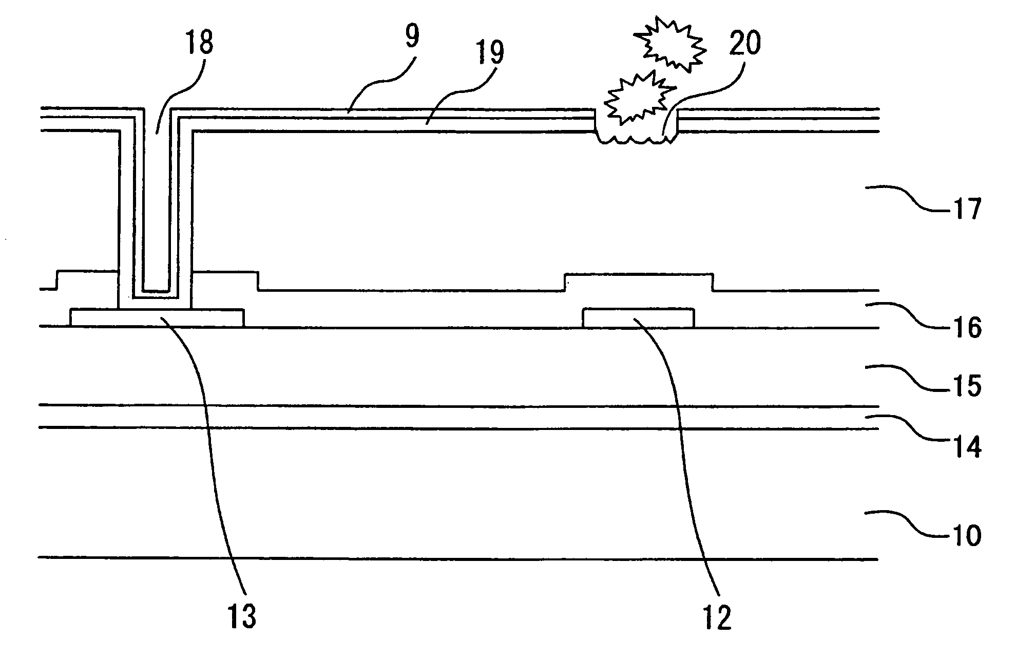
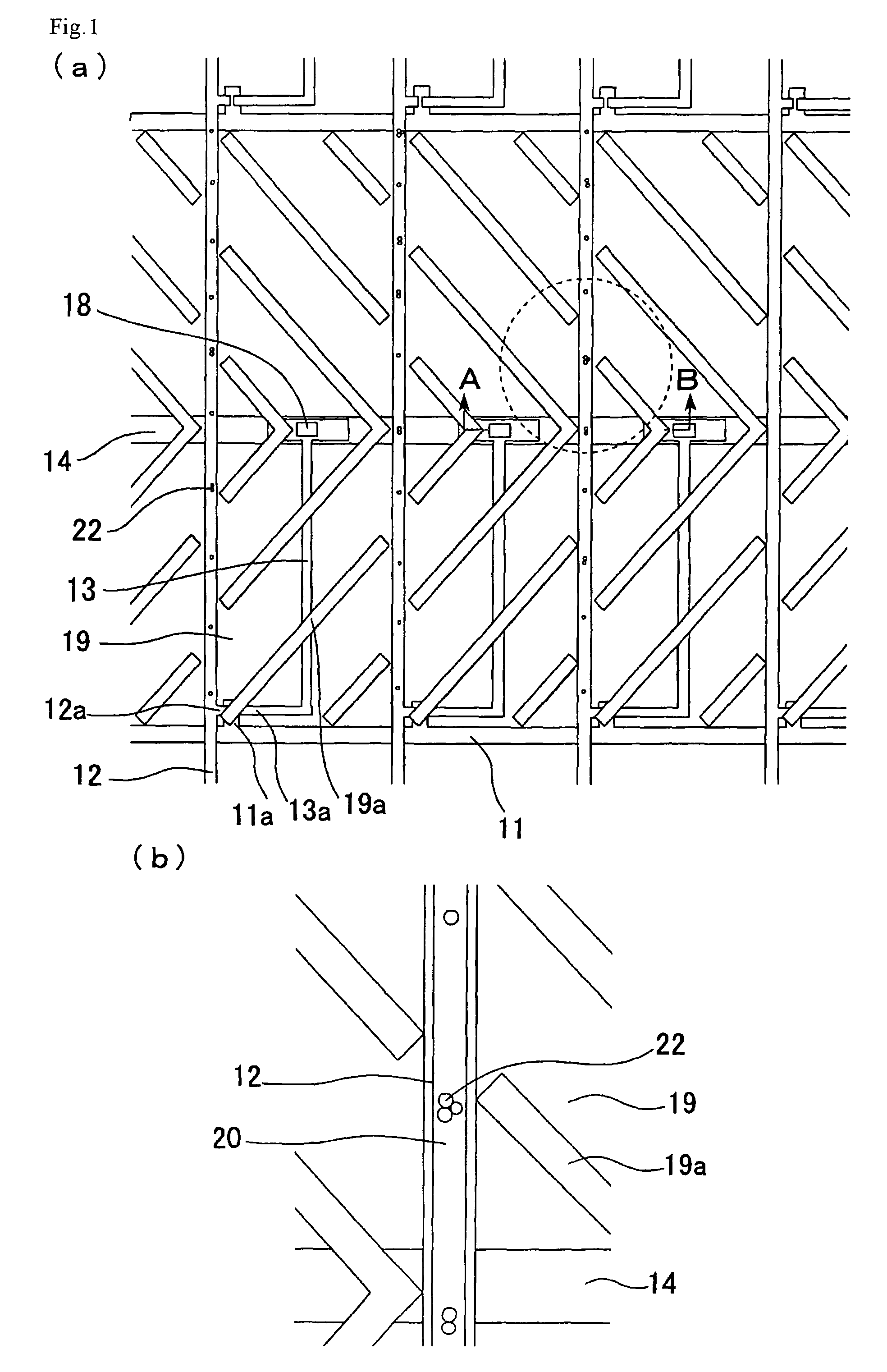
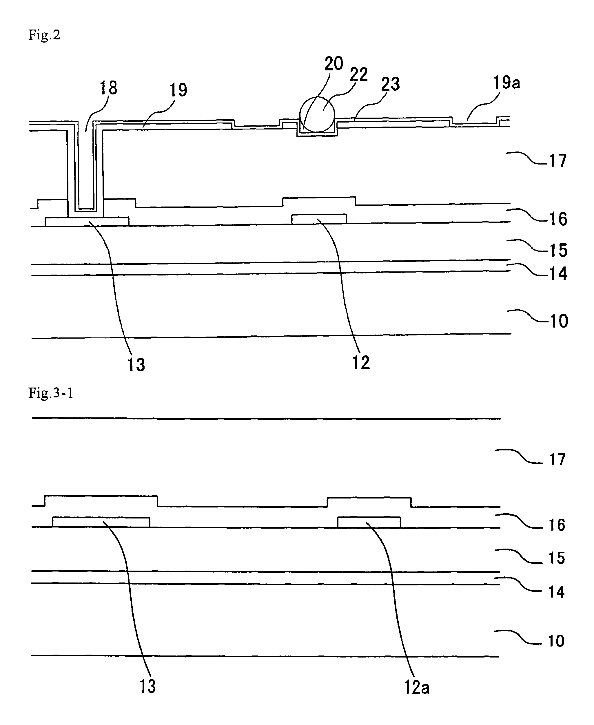
[0054]FIG. 1(a) is a planar view schematically showing a configuration of a TFT array substrate mounted on a liquid crystal display panel, in accordance with one embodiment of the present invention. FIG. 1(b) is an enlarged view schematically showing a region surrounded by the circle (dotted line) of the TFT substrate shown in FIG. 1(a). FIG. 2 is a cross-sectional view schematically showing the TFT array substrate taken along line A-B in FIG. 1(a).
[0055]In the TFT array substrate according to the present embodiment, as shown in FIG. 1(a), a gate wiring 11 and a source wiring 12 are disposed to intersect with each other. At the intersection, a TFT as a switching element and an ITO (indium tin oxide) pixel electrode 19 are disposed. The TFT has a bottom gate structure in which a source electrode 1...
embodiment 2
[0078]A production method of a TFT array substrate in accordance with Embodiment 2 as another embodiment of the multilayer substrate of the present invention is mentioned.
(1) Production of TFT Array Substrate
(1-1) Formation of Gate Wiring 11 (11a) to Formation of Protective Film 16
(1-2) Coating of Resin Interlayer Insulating Film 17
(1-1) and (1-2) are the same as those in Embodiment 1, and therefore the explanation thereof is omitted.
(1-3) Exposure and Development of Resin Interlayer Insulating Film 17 and Etching of Protective Film
[0079]FIGS. 4-1 and 4-2 are cross-sectional views schematically showing a step of exposing and developing the resin interlayer insulating film 17 and a step of etching the protective film 16, respectively.
[0080]The present Embodiment is the same as (1-3) of Embodiment 1, except that only the partial contact hole was formed using a mask 8 having only a specific transmission pattern 8c (FIGS. 4-1 and 4-2).
(1-4) Formation of ITO Pixel Electrode 19
[0081]FIG. ...
embodiment 3
[0089]A configuration of a color filter (CF) substrate of Embodiment 3 as one example of the multilayer substrate of the present invention is mentioned.
[0090]FIG. 6 is a planar view schematically showing a configuration of a CF substrate mounted on a liquid crystal display panel in accordance with one embodiment of the present invention. FIG. 7 is a cross-sectional view schematically showing the CF substrate taken along line C-D in FIG. 6.
[0091]In the CF substrate according to the present embodiment, as shown in FIG. 6, a colored layer (color layer) 31 and a black matrix (BM, color layer) 32 were each disposed on a glass substrate 30 in a stripe pattern, and as shown in FIG. 7, an overcoat layer (resin interlayer film) 37 and an ITO electrode 39 were formed to cover the colored layer 31 and the black matrix 32. As mentioned above, the overcoat layer 37 was formed between the colored layer 31 and the like, and the ITO electrode 39 in order to planarize the CF substrate surface.
[0092]...
PUM
| Property | Measurement | Unit |
|---|---|---|
| depth | aaaaa | aaaaa |
| depth | aaaaa | aaaaa |
| depth | aaaaa | aaaaa |
Abstract
Description
Claims
Application Information