Inductor

a technology of inductors and inductors, applied in the direction of transformers/inductors, inductances, inductance coils/windings/connections, etc., can solve the problems of low effective capacitance between adjacent track sections, and the generality of semiconductor manufacturing techniques that do not allow features with curves, so as to prevent electrical shorting

Active Publication Date: 2012-06-19
NXP BV
View PDF2 Cites 5 Cited by
  • Summary
  • Abstract
  • Description
  • Claims
  • Application Information

AI Technical Summary

Benefits of technology

[0023]The claimed invention allows an inductor to be provided, which has reduced parasitic capacitance between the inductor turns thereof, without substantially affecting the inductors self inductance (the self inductance of the inductor is substantially independent of the configuration of the crossing points therein). The reduction in parasitic capacitance is a consequence of the novel arrangement of the track sections, which make up the inductor turns. In particular, the crossing over of the track sections at the group of crossing points causes adjacent track sections in the inductor to have a lower potential difference between them (assuming there is a voltage drop along the length of the conductive track), which in turn leads to a lower effective capacitance between adjacent track sections. Summed over all adjacent track sections in the inductor, the parasitic capacitance is lower than for known inductors. The reduction in parasitic capacitance can lead to an increase in resonant frequency and Q-factor.
[0026]In accordance with an embodiment of the invention, the crossing points of at least one group of crossing points can be located together in a common portion of the inductor. This collocation of the crossing points ensures that overlap between adjacent track sections in the inductor having reduced potential difference there-between is maximised, whereby the benefit of reducing the parasitic capacitance between adjacent track sections is also maximised. If the crossing points were distributed throughout the inductor, at least some adjacent track sections would have a higher potential difference there-between, and consequently the overall parasitic capacitance between the turns in the inductor would be increased.
[0029]In one embodiment, each crossing point can include insulation for electrically isolating the conductive track, to prevent electrical shorting between the track sections.

Problems solved by technology

In particular, the crossing over of the track sections at the group of crossing points causes adjacent track sections in the inductor to have a lower potential difference between them (assuming there is a voltage drop along the length of the conductive track), which in turn leads to a lower effective capacitance between adjacent track sections.
However, semiconductor manufacturing techniques do not generally allow for features having curves, and instead straight lines must be used.

Method used


Image

  • Inductor
  • Inductor
  • Inductor

Examples


first embodiment

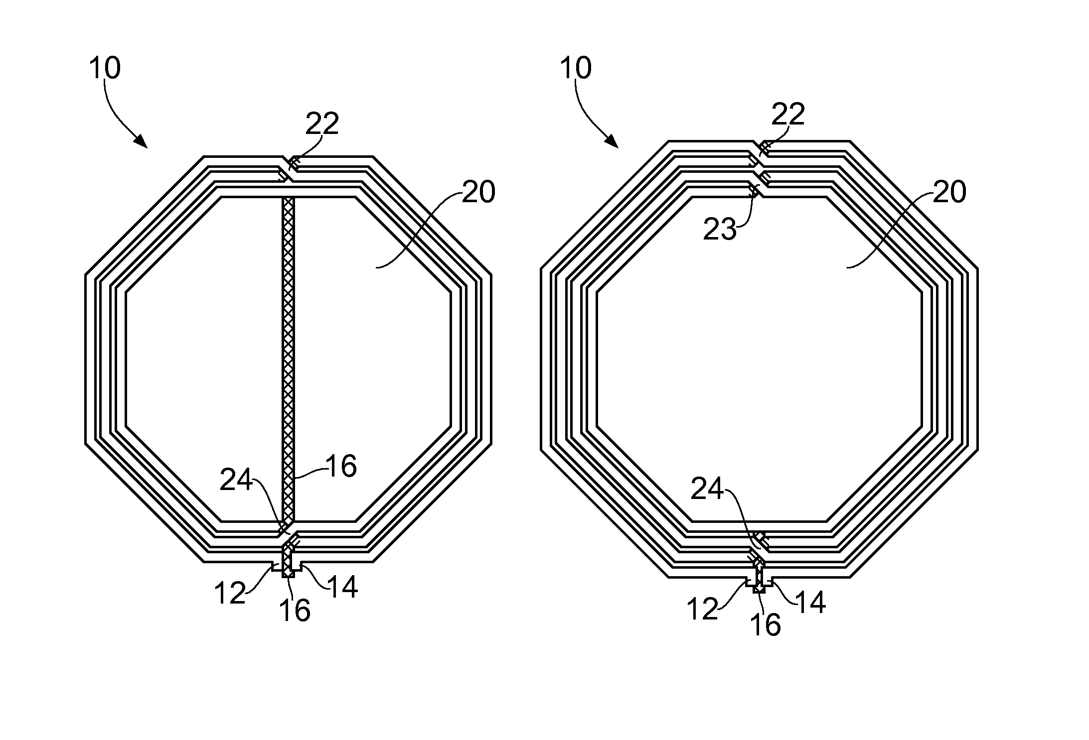
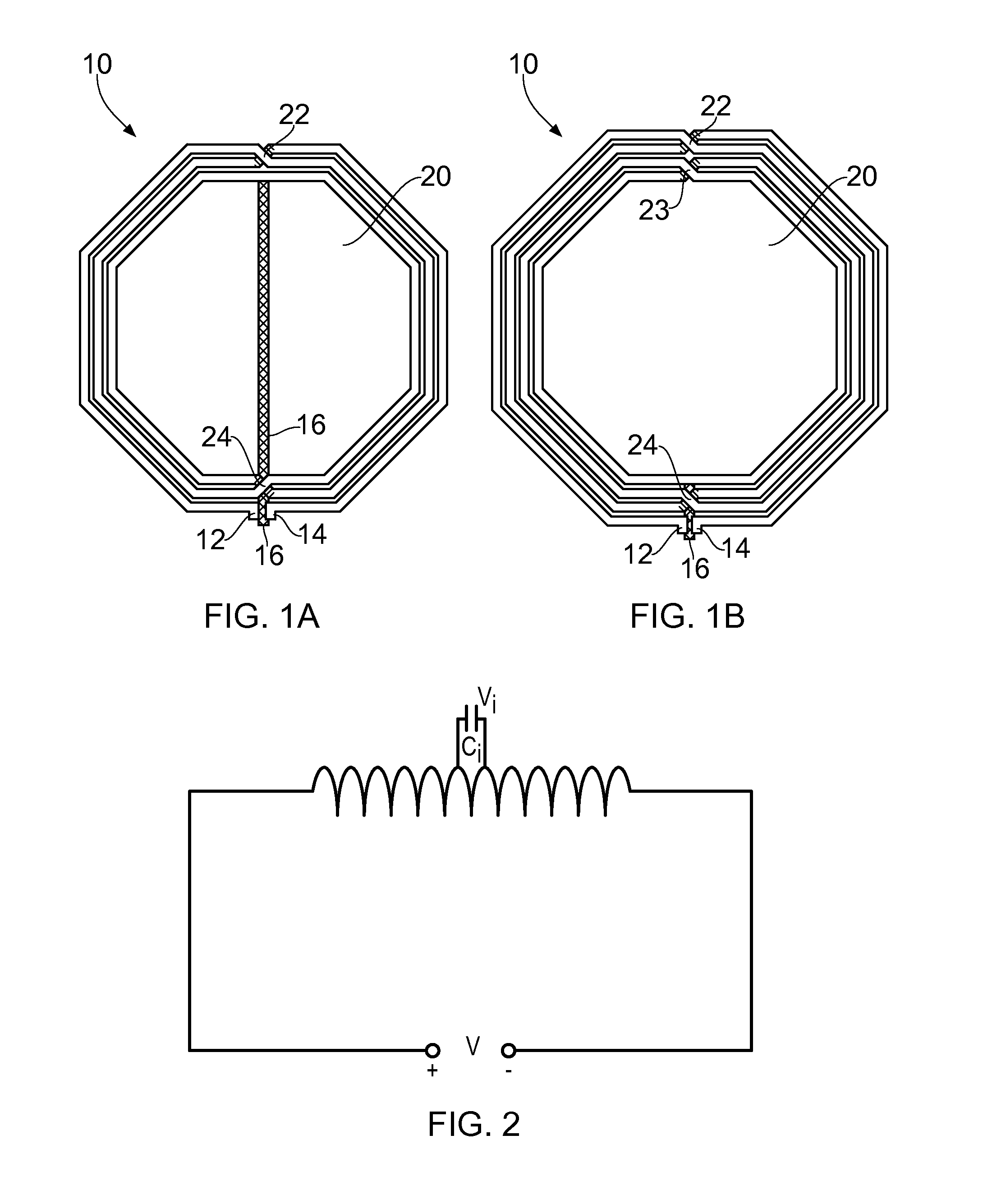
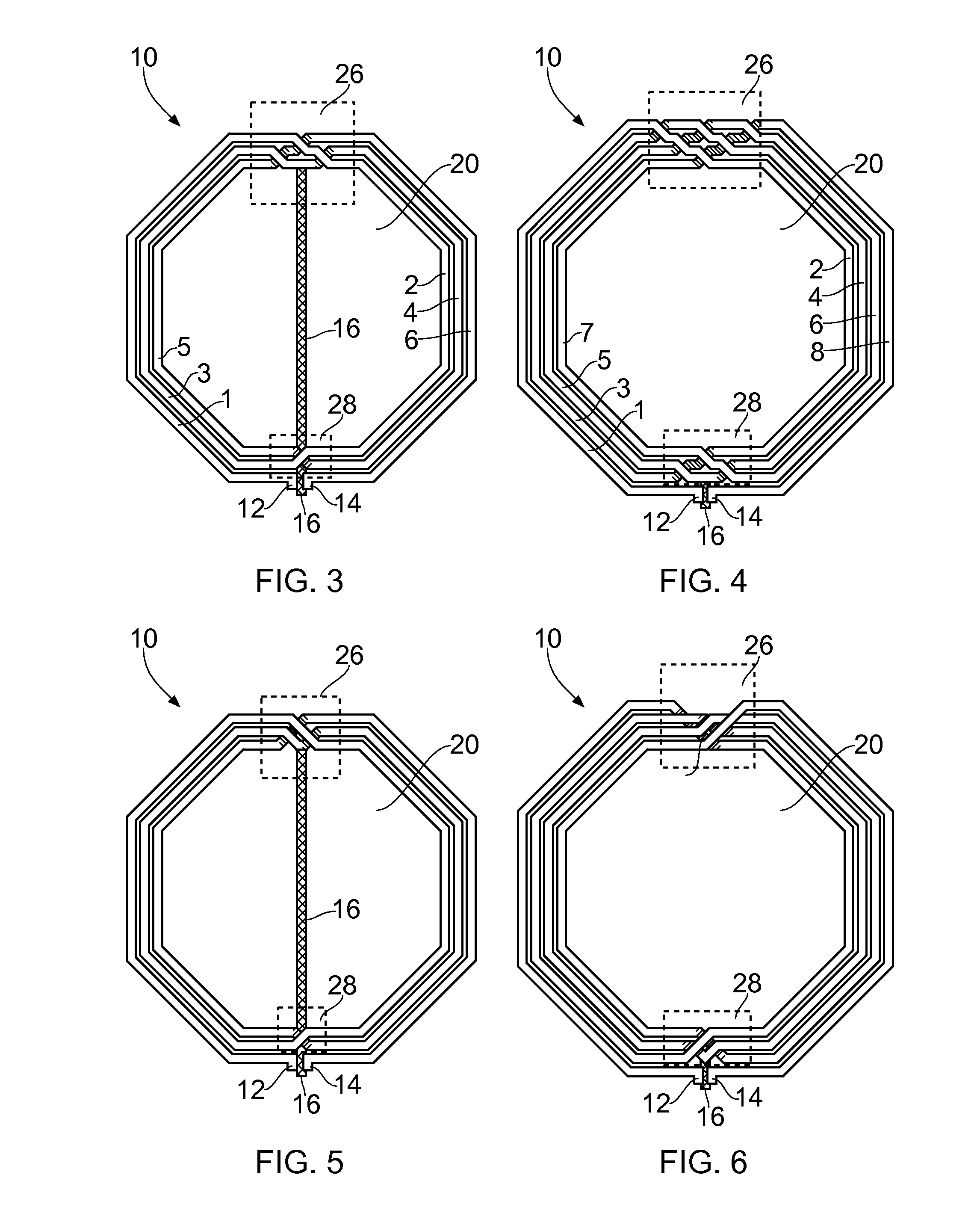
[0051]the invention is illustrated in FIG. 3. In this embodiment, there is provided a three turn inductor 10. The inductor 10 includes a conductive track which extends between conductor terminals 12 and 14 to form the three windings. In this example, the inductor is substantially symmetrical and substantially octagonal, although these features are not essential to the invention. For example, the inductor may not be exactly symmetrical, and shapes other than an octagon may be employed (e.g. square, hexagonal). Nevertheless, the substantially symmetrical configuration of the windings of the inductor allow the appropriate inclusion of a centre tap 16 as shown in FIG. 3. Moreover, the octagonal configuration of the inductor complies with known design rules for semiconductor manufacturing processes.

[0052]In this example, the inductor 10 includes six track sections (1, 2, 3, 4, 5, 6). Each track section comprises a portion of the conductive track which extends between a first group 26 of ...

second embodiment

[0059]The principal of providing a group of crossing points to reverse the order of the track sections in the inductor can be applied to inductors having any number (n) of inductor turns, where n is at least 3. Thus, for example, FIG. 4 illustrates the invention, in which there is provided an inductor 10 having n=4 inductor turns. The inductor 10 in FIG. 4 includes similar features to those described above in relation to FIG. 3 (terminals 12 and 14, a centre tap 16, a first group 26 of crossing points and a second group 28 of crossing points). As the inductor 10 in FIG. 4 has four windings, eight track sections (1, 2, 3, 4, 5, 6, 7, 8) are present.

[0060]As with FIG. 3, at the first group 26 of crossing points, the order of the track sections in the inductor is reversed such that inner track sections of the conductive track cross-over to become respective outer track sections, and such that outer track sections of the conductive track cross-over to become respective inner track secti...


PUM

PropertyMeasurementUnit
widthaaaaaaaaaa
widthaaaaaaaaaa
inner diameteraaaaaaaaaa

Abstract

An inductor includes a conductive track forming at least three inductor turns. The conductive track has a plurality of track sections. The inductor also includes at least two groups of crossing points, each crossing point comprising a location at which the conductive track crosses over itself. The crossing points of each group collectively reverse the order of at least some of the track sections in the inductor, such that inner track sections of the conductive track cross over to become respective outer track sections, and such that outer track sections of the conductive track cross over to become respective inner track sections.

Description

[0001]This application claims the priority under 35 U.S.C. §119 of European patent application no. 09180111.8, filed on Dec. 21, 2009, the contents of which are incorporated by reference herein.BACKGROUND OF THE INVENTION[0002]This invention relates to an inductor.[0003]It is well known to provide spiral inductors to realise devices such as voltage controlled oscillators (VCOs) in, for example, a transceiver in an integrated circuit (IC).[0004]An inductor can be characterised, inter alia, in terms of its resonant frequency ω, which is a function of the self inductance L of the inductor, and the parasitic capacitance C of the inductor:[0005]ω=1LC(1)Another characteristic of an inductor is its Quality factor (Q-factor):[0006]Q=ω⁢⁢LR(2)where R is the internal resistance of the inductor, and ωL is the inductive resistance of the inductor.[0007]From equation (1), it can be seen that the resonant frequency of an inductor can be increased by minimising the parasitic capacitance. There are ...

Claims


Application Information

Patent Timeline
Patent Type & Authority Patents(United States)
IPC IPC(8): H01F5/00
CPCH01F5/003H01F17/0006H01F27/2804H01F27/34H01F21/12H01F2017/0073
Inventor NAZARIAN, ALEXE LEVANTIEMEIJER, LUKAS FREDERIK
Owner NXP BV
Why Eureka
Try Eureka