Device and method for reading electric currents resulting from an electromagnetic signal detector

a technology of electromagnetic signal and detector, which is applied in the field of devices for reading electric currents, can solve the problems of photo-detectors that generally consume as little power as possible, have very short reaction and integration times, and have very short reaction and integration times, and achieve the effect of reducing the time needed to reset, and reducing the number of times of operation

Active Publication Date: 2012-07-10
DE DETECTEURS INFRAROUGES - SOFRADIR
View PDF14 Cites 0 Cited by
  • Summary
  • Abstract
  • Description
  • Claims
  • Application Information

AI Technical Summary

Benefits of technology

[0043]The object of the present invention is therefore a device for reading electric currents, and particularly those coming from elementary matrix sensors, that has a relatively stable potential difference at the terminals of the elementary sensors, restricts the injection of parasitic charges into the integration circuit, is relatively small in bulk, does not consume much energy, is not prone to overheating, is fairly insensitive to blooming, and has good linearity and a high signal-to-noise ratio.
[0051]Such transistors allow the current reading device to perform well, particularly in terms of response time linearity or power consumption.
[0053]Said feature allows the linearity of the input stage of a matrix photo-detector to be increased. In addition, this structure can be used to achieve multi-integration, in other words a time slicing of the integration windows between two reading resets.
[0063]According to one embodiment of the invention, the amplitudes of the first and second pulses are selected in such a way that a transistor put into the off state is on the verge of triggering the on state. In this way, the second transistor unblocks without greatly depolarizing the detector if the first transistor is no longer able to drain the charges coming from the elementary sensors. An effective anti-blooming function is thus implemented.

Problems solved by technology

Apart from this constraint on bulk which is crucial, photo-detectors must generally consume as little power as possible and have very short reaction and integration times. The power consumption problem proves particularly significant in the case of cooled photo-detectors, such as diode detectors for the infrared radiation spectrum for example.
The input stages shown in FIGS. 1 and 2 have furthermore the drawback of being sensitive to bloom, which even so causes the sensor to depolarize or a parasitic current to appear in the multiplexing system.
However, adding components of this kind, and in particular the capacitive element 407, necessarily increases the bulk of the read device, as well as its power consumption.
However, sizing the components 406 and 407 in this way causes a degradation of the wanted signal, in other words of the integrated current, since there is dilution of the wanted signal, increase in noise and injection of non-linear charges in the transistor 406.
Such a degradation of the wanted signal inevitably involves a decrease in the signal-to-noise ratio, and therefore in the performance of the photo-detector provided with an input stage of this kind.
First of all, there is instability in sensor polarization, under the effect of the polarization voltage pulses.
But the input stage as shown in FIG. 5 does not allow a stable potential to be maintained at the terminals of the elementary sensor, when the polarization transistor is in the off state, in other words outside the integration phase.
Consequently, prior art input stages that use polarization transistor blocking cannot prevent the integration of parasitic charges into the capacitance, parasitic charges inevitably carried by the diode constituting the elementary sensor.
Quite obviously, such parasitic charges cause a drift in potential difference at the terminals of the elementary sensor and, consequently, degrade the linearity which constitutes an essential performance element in rating any photo-detector.
Consequently, as is the case in respect of sampling, this architecture has the drawback of degrading the linearity of the wanted signal.
These two drawbacks are particularly disadvantageous if the circuit is to be used defining a plurality of integration windows between two resets of the integrating capacitance.

Method used


Image

  • Device and method for reading electric currents resulting from an electromagnetic signal detector
  • Device and method for reading electric currents resulting from an electromagnetic signal detector
  • Device and method for reading electric currents resulting from an electromagnetic signal detector

Examples


Embodiment Construction

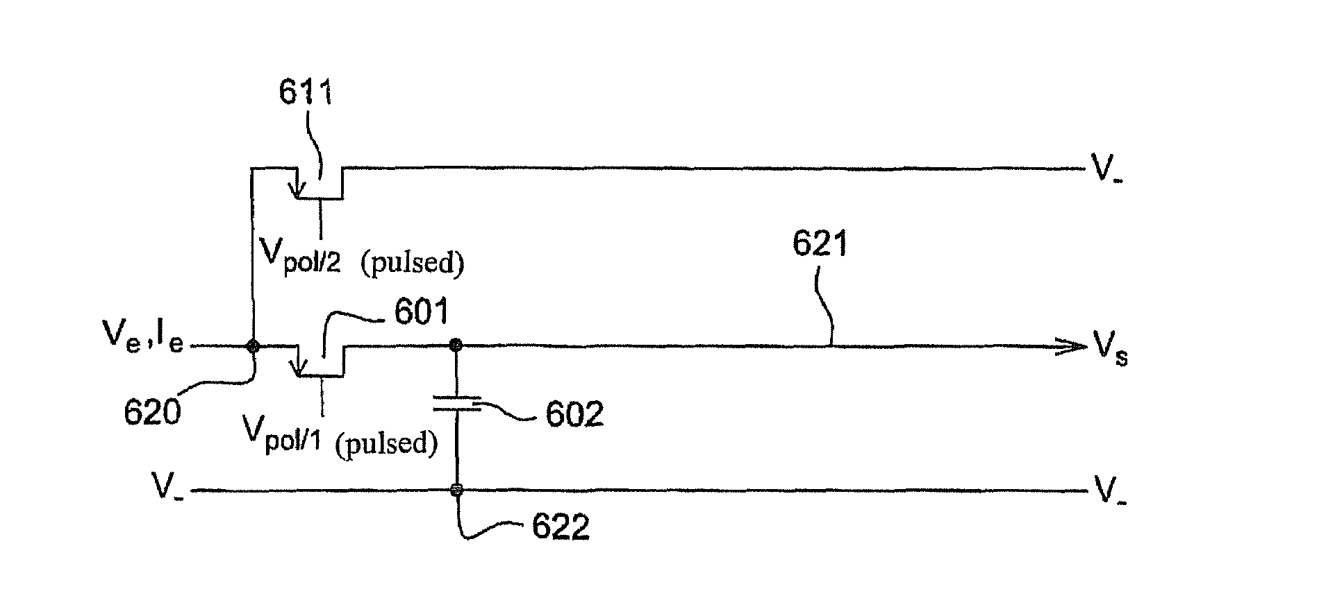
[0069]FIG. 6 thus shows an input stage in accordance with an embodiment of the present invention.

[0070]In this input stage, two p-type MOS transistors 601 and 611 produced using CMOS technology are implanted in order to define a differential pair. The first and second transistors 601 and 611 are therefore mounted on two parallel branches, and have node 620 as a tie point, into which is injected the current for reading Ie, which represents the input current coming from a sensor, such as a photodiode.

[0071]According to the invention, the source of the first transistor 601 is connected to the input branch intended to inject the current Ie for reading. The drain of the first transistor 601 is itself connected to the output branch, by means of a node 621. The node 621 is therefore brought to the potential Vs, representing the output voltage.

[0072]In accordance with the invention, the gate of the first transistor 601 is connected to a polarized impulse voltage source (not shown), capable ...


PUM


Abstract

A device for reading electric currents including a capacitive element to integrate the current, the terminals of the capacitive element being connected to the mass and to an output branch of the device respectively, and a differential pair including: a first transistor mounted between the input branch of the input stage and the capacitive element, the transistor being controlled by a polarized impulse voltage, capable of putting the first transistor alternately into the off state and then into the on state; and a second transistor mounted between the input branch of the input stage and a potential other than that of the capacitive element, said transistor also being controlled by a polarized impulse voltage, capable of putting the second transistor alternately into the off state and then into the on state, wherein the second transistor is mounted in phase opposition relative to the first transistor.

Description

FIELD OF THE INVENTION[0001]The present invention relates to the field of the design of integrated circuits for reading the current coming from a sensor during an integration time in order to store the relevant charges in a capacitor.[0002]The present invention relates more particularly to a device for reading electric currents, such as those generated in the elementary sensors of a matrix photo-detector during the interactions between photons and matter. In particular, the device constituting the object of the present invention may be used to convert the analog quantities produced by infrared detectors, and more particularly cooled bolometric detectors, into digital values.[0003]The present invention also relates to a method for reading electric currents employed by the device constituting the object of the invention.BACKGROUND OF THE INVENTION[0004]Generally speaking, to read the electric current coming from a sensor, a two-phase method needs to be adopted, namely:[0005]an integra...

Claims


Application Information

Patent Timeline
Patent Type & Authority Patents(United States)
IPC IPC(8): G01R1/00H04N5/378
CPCG01J1/46H04N5/378H04N25/75
Inventor SANSON, ERIC
Owner DE DETECTEURS INFRAROUGES - SOFRADIR
Why Eureka
Try Eureka