
Method for purifying metallurgical silicon for solar cells

a technology of metallurgical silicon and solar cells, applied in the field of apparatus and methods for purifying materials, can solve problems such as limitations of conventional methods, and achieve the effect of reducing costs

Active Publication Date: 2012-08-07
HOSHINO MASAHIRO +1
View PDF17 Cites 6 Cited by
  • Summary
  • Abstract
  • Description
  • Claims
  • Application Information

AI Technical Summary

Benefits of technology

"The present invention provides a system and method for purifying metallurgical silicon fields to produce high-quality silicon for solar cells. The invention addresses limitations of conventional methods by using a crucible made of quartz material and capable of withstanding high temperatures. The system includes an energy source, such as an arc heater, to melt the raw silicon material in a crucible. The melted material is then purified by removing impurities, such as phosphorus, to produce high-quality silicon. The purification process involves subjecting the melted material to a temperature profile that causes the phosphorus to form a determined temperature profile while maintaining the outer regions of the melted material at a lower temperature. The purification process also includes a convective flow caused by the temperature gradient formed by the temperature profile. The invention provides a cost-effective solution for producing high-quality silicon for solar cells."

Problems solved by technology

But with increasing demands for cleaner and more flexible production, lower cost, and mass production capability, the conventional method has limitations.

Method used

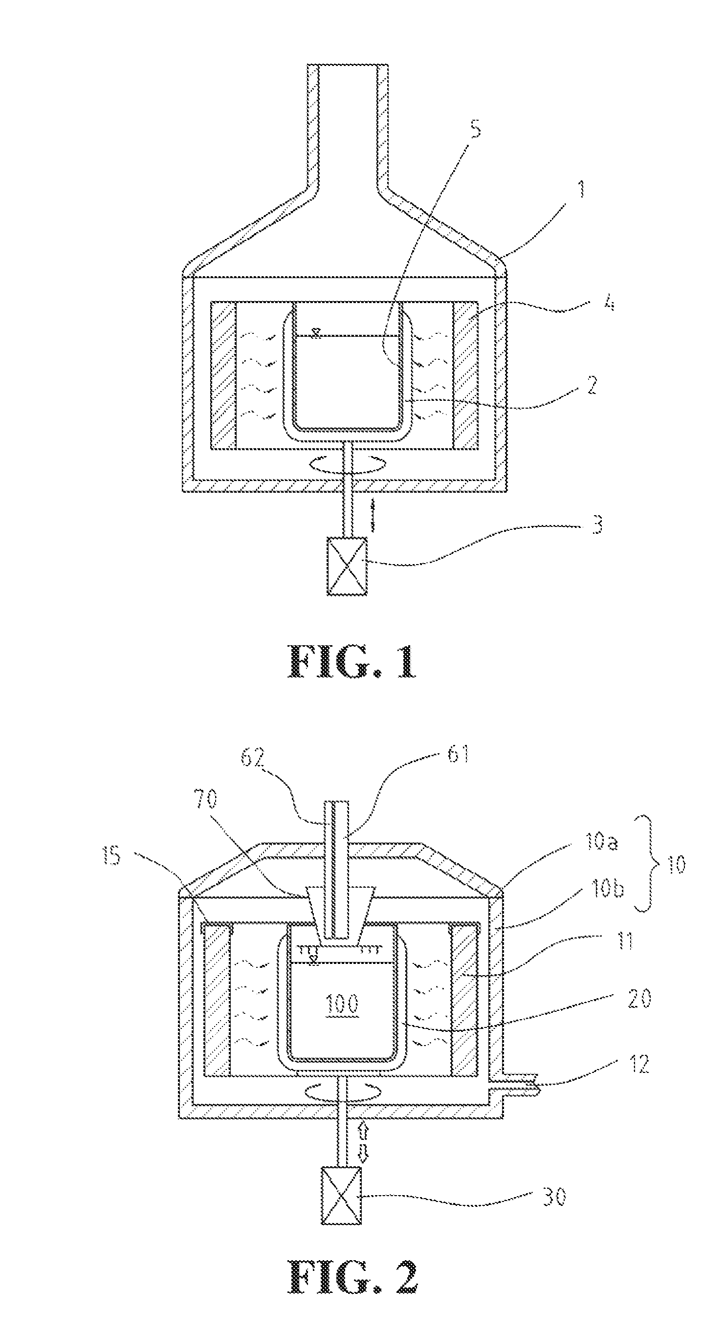
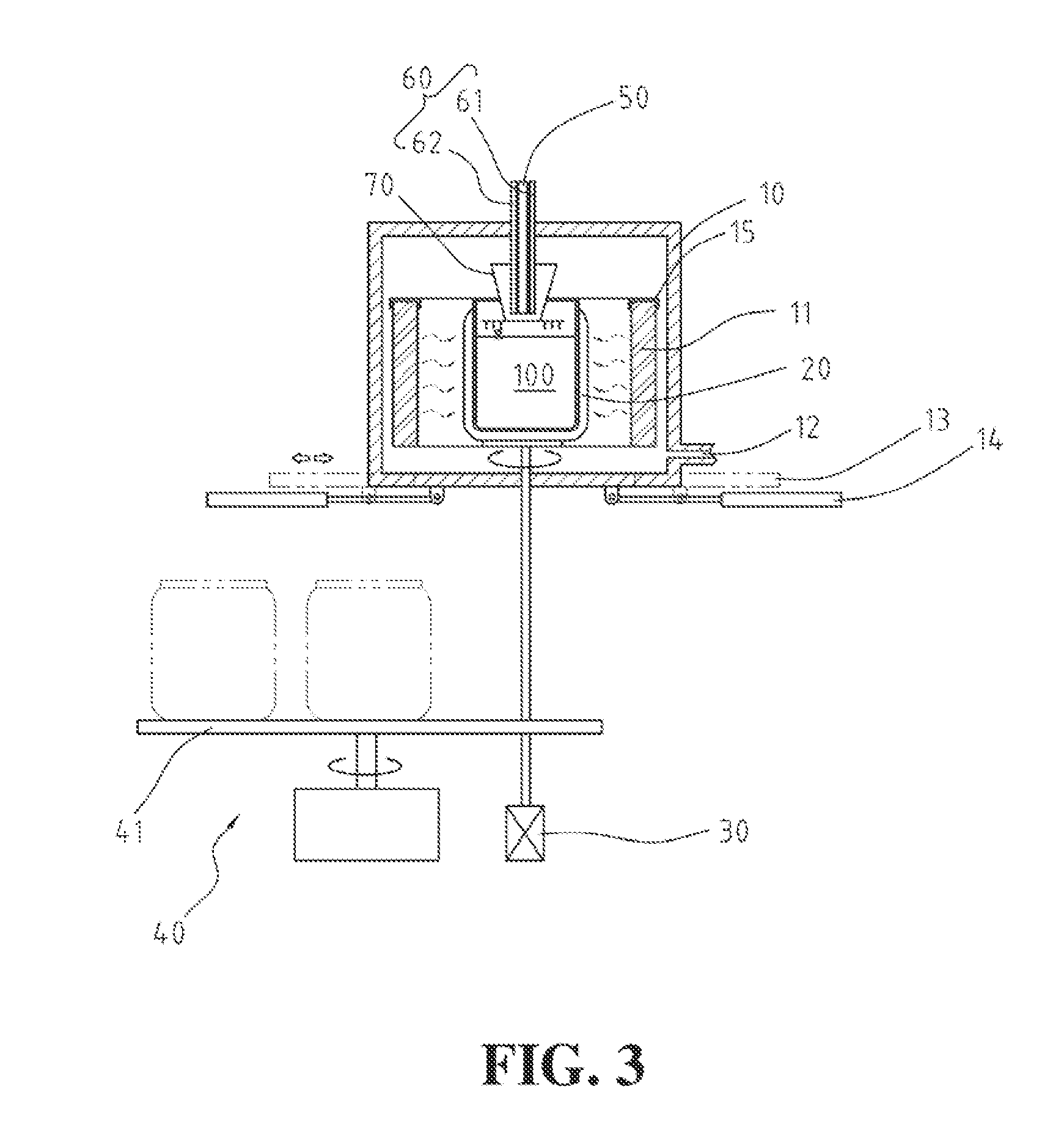

Image

  • Method for purifying metallurgical silicon for solar cells
  • Method for purifying metallurgical silicon for solar cells
  • Method for purifying metallurgical silicon for solar cells

Examples


example

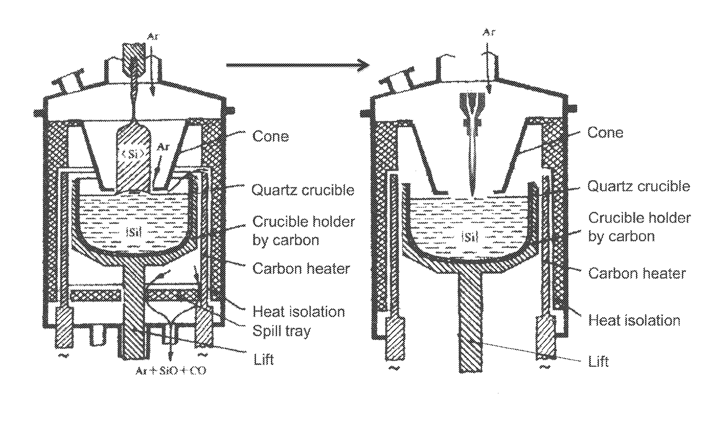
[0122]To prove the principle and operation of the present invention, we performed certain experiments. We performed the poly-Si purification experiments using several generations of modified conventional single crystal Si ingot pullers. Such pullers included a very small and conventional puller (about 20 Kg Si per charge) to a mid-size puller (about 80 Kg Si per charge). We maintained the crucible apparatus and controls, which were modified to operate in a manner consistent with the present pilot silicon purification apparatus configured for purifying metallurgical silicon. Upon introducing metallurgical silicon, processing such silicon, and purifying the silicon according to the present examples. We achieved purification result of 6N˜7N (e.g., 99.9999 to 99.99999 silicon purity), reaching the desired specification suitable for solar cell applications. The present pilot purifier in operation has been modified from a large size conventional puller (about 140 Kg Si per charge). See, f...


PUM

PropertyMeasurementUnit
temperatureaaaaaaaaaa
depthaaaaaaaaaa
flow rateaaaaaaaaaa

Abstract

The present invention provides a method for forming high quality silicon material, e.g., polysilicon. The method includes transferring a raw silicon material in a crucible having an interior region. The crucible is made of a quartz or other suitable material, which is capable of withstanding a temperature of at least 1400 Degrees Celsius. The method includes subjecting the raw silicon material in the crucible to thermal energy to cause the raw silicon material to be melted into a liquid state to form a melted material at a temperature of less than about 1400 Degrees Celsius. Preferably, the melted material has an exposed region bounded by the interior region of the crucible. The method also includes subjecting an exposed inner region of the melted material to an energy source comprising an arc heater configured above the exposed region and spaced by a gap between the exposed region and a muzzle region of the arc heater to cause formation of determined temperature profile within a vicinity of an inner region of the exposed melted material while maintaining outer regions of the melted material at a temperature below a melting point of the quartz material of the crucible. Preferably, the method removes one or more impurities from the melted material to form a higher purity silicon material in the crucible.

Description

CROSS REFERENCE TO RELATED APPLICATIONS[0001]This application claims priority to U.S. Ser. No. 61 / 374,213 filed on Aug. 16, 2010, U.S. Ser. No. 13 / 023,467 filed on Feb. 8, 2011 and Republic of China Patent Application No. 099104551 filed on Feb. 12, 2010, commonly assigned, and hereby incorporated by reference herein.BACKGROUND OF THE INVENTION[0002]The present invention relates to an apparatus and method for purifying materials. More particularly, the present invention relates to a method and system for purifying metallurgical silicon fields to produce raw materials suitable for manufacturing single crystal silicon ingots and poly crystal silicon ingots for solar cells at a lower cost. Although the above has been described in terms of purifying silicon, it can be applied to other applications.[0003]Conventional polysilicon silicon material used for manufacturing solar cells is often produced by the so-called Siemens process. Such process is well established, stable, and produces si...

Claims


Application Information

Patent Timeline
Patent Type & Authority Patents(United States)
IPC IPC(8): C01B33/02C01B33/021
CPCC01B33/037C30B11/002C30B11/003C30B29/06F27B14/06F27B14/14H05B7/18Y02E10/546
Inventor HOSHINO, MASAHIROKAO, CHENG C.
Owner HOSHINO MASAHIRO
Learn More