Semiconductor device with liquid repellant layer

a technology of liquid repellant layer and semiconductor device, which is applied in the direction of solid-state device, basic electric element, thermoelectric device, etc., can solve the problems of rising writing voltage and not flowing current easily, and achieve the effect of low writing voltage and low cos

Inactive Publication Date: 2012-08-14
SEMICON ENERGY LAB CO LTD
View PDF45 Cites 4 Cited by
  • Summary
  • Abstract
  • Description
  • Claims
  • Application Information

AI Technical Summary

Benefits of technology

[0005]Therefore, it is also an object of the present invention to provide technology for manufacturing a higher-reliability memory device and semiconductor device at low cost by lowering the writing voltage.
[0008]The region having a different wettability is a region having a difference in wettability against the fluid composition, and where the contact angle of the fluid composition is different. A region where the contact angle of the fluid composition is large is a region with low wettability (hereinafter also referred to as a low wettability region), and a region where the contact angle is small is a region with high wettability (hereinafter also referred to as a high wettability region). When the contact angle is large, the fluid composition does not wet a region surface because it is repelled and does not expand on the surface. On the other hand, when the contact angle is small, the fluid composition expands on the surface, and wets the surface well. Therefore, the region with the different wettability is also different in surface energy. The surface energy of a region with low wettability is low, and the surface energy of a region with high wettability is high.
[0010]Note that in the present invention, a semiconductor device refers to a device that can function by utilizing a semiconductor characteristic. By using the present invention, it is possible to manufacture a semiconductor device such as a chip having a processor circuit (hereinafter also referred to as a processor chip), and the like.
[0011]One aspect of a semiconductor device of the present invention is to have a first conductive layer, a first insulating layer that is in contact with a side end portion of the first conductive layer, a second insulating layer over the first conductive layer and the first insulating layer, and a second conductive layer over the second insulating layer. The second insulating layer is formed of an insulating material, and the wettability against a fluidized substance when the insulating material is fluidized, is higher for the first insulating layer than the first conductive layer.
[0014]By the present invention, a higher-reliability semiconductor device having lower writing voltage can be manufactured at low cost.

Problems solved by technology

However, in a memory circuit using an organic compound in which a memory element is formed by providing an organic compound between a pair of electrodes, current does not flow easily depending on the thickness of the organic compound layer or the size of the memory circuit, and thus the rise in writing voltage becomes a problem.
Therefore, an insulating layer made of the substance containing an insulating material becomes a fluid composition at or over the glass-transition temperature and does not maintain a constant form, and behaves like a liquid.

Method used


Image

  • Semiconductor device with liquid repellant layer
  • Semiconductor device with liquid repellant layer
  • Semiconductor device with liquid repellant layer

Examples


embodiment mode 1

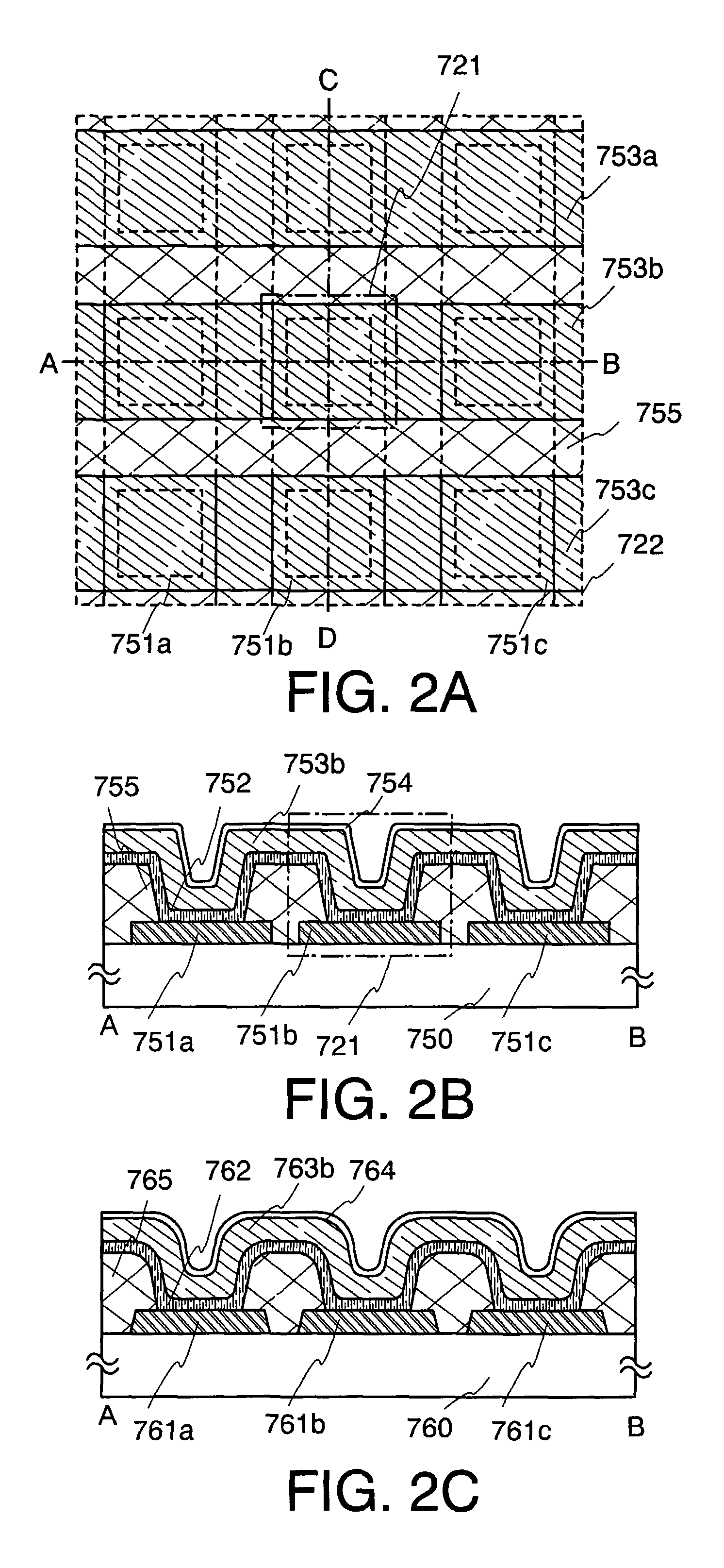
[0036]In this embodiment mode, one example of a structure of a memory element included in a memory device of the present invention will be described with reference to drawings. More specifically, a case where the structure of a memory device is a passive matrix type will be described.

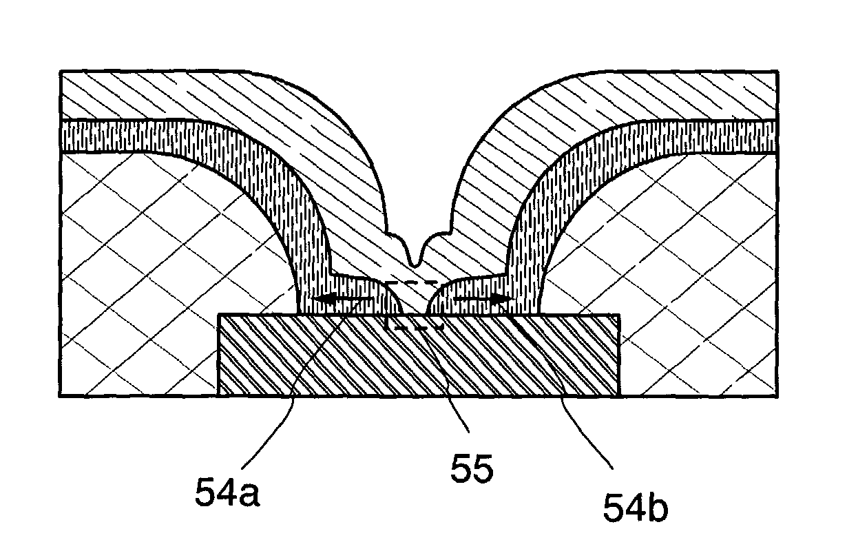
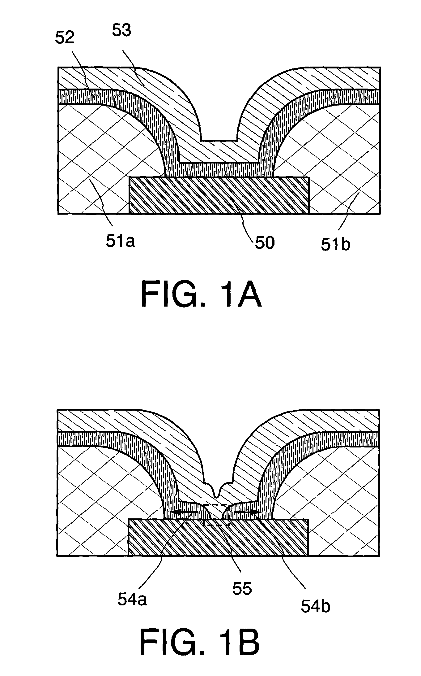
[0037]A memory element of the present invention and an operation mechanism thereof will be described with reference to FIGS. 1A and 1B. In FIGS. 1A and 1B, a partition (insulating layer) 51a and a partition (insulating layer) 51b are provided so as to cover the end portions of a first conductive layer 50. The partitions (insulating layers) 51a and 51b also serve as partitions to separate a memory element from other memory elements. Then, an insulating layer 52 is formed over the partitions (insulating layers) 51a and 51b, and the first conductive layer 50. Furthermore, a second conductive layer 53 is formed over the insulating layer 52.

[0038]As materials for the first conductive layer 50 and the second ...

embodiment mode 2

[0097]In this embodiment mode, a memory device having a structure different from that of the above embodiment mode 1 is described. Specifically, a case where the structure of a memory device is an active matrix type is described.

[0098]FIG. 5 shows an example of a structure of the memory device that is described in this embodiment mode, which includes a memory cell array 232 in which memory cells 231 are provided in a matrix form; a bit line driving circuit 226 that has a column decoder 226a, a readout circuit 226b, and a selector 226c; a word line driving circuit 224 that has a row decoder 224a and a level shifter 224b; and an interface 223 which carries out interactions with the exterior and has a writing circuit and the like. Note that the structure of a memory device 216 shown here is only one example, and it may include another circuit such as a sense amplifier, an output circuit, or a buffer, and the writing circuit may be provided in the bit line driving circuit.

[0099]A single...

embodiment mode 3

[0115]In this embodiment mode, one example of a semiconductor device having the memory device shown in the above mentioned embodiment mode, will be described with reference to drawings.

[0116]A characteristic of the semiconductor device shown in this embodiment mode is that data readout and writing are possible without contact. Data transmission methods are classified broadly into three, and any of the following may be used: an electromagnetic coupling method of communicating by mutual induction with a pair of coils placed opposite of each other; an electromagnetic induction method of communicating by an inductive electromagnetic field; or an electric wave method of communicating by using electric waves. Also, an antenna that is used for transmitting data can be provided in two ways. One way is to provide the antenna over a substrate over which a plurality of elements and memory elements are formed; and the other way is to provide a terminal portion for a substrate over which a plura...


PUM


Abstract

An object is to provide technology for manufacturing a higher-reliability memory device and a semiconductor device that is equipped with the memory device at low cost. A semiconductor device of the present invention has a first conductive layer, a first insulating layer that is provided to be in contact with a side end portion of the first conductive layer, a second insulating layer that is provided over the first conductive layer and the first insulating layer, and a second conductive layer that is provided over the second insulating layer. The second insulating layer is formed of an insulating material, and wettability against a fluidized substance when the insulating material is fluidized, is higher for the first insulating layer than the first conductive layer.

Description

TECHNICAL FIELD[0001]The present invention relates to a semiconductor device and a manufacturing method of a semiconductor device.BACKGROUND ART[0002]In recent years, object recognition technology which can be useful in production, management, etc., by assigning IDs (identification numbers) to individual objects and keeping their accurate track records, has attracted much attention. Further, semiconductor devices that can send and receive data without contact have been in development. As such semiconductor devices, RFIDs (abbreviation of Radio Frequency Identification; also referred to as ID tags, IC tags, IC chips, RF tags (Radio Frequency), wireless tags, electronic tags, and wireless chips) and the like are beginning to be adopted within companies, markets, and the like.[0003]Many of these semiconductor devices each includes an antenna, and a circuit (hereinafter also referred to as IC (Integrated Circuit) chips) using a semiconductor substrate of silicon (Si) or the like, in whi...

Claims


Application Information

Patent Timeline
Patent Type & Authority Patents(United States)
IPC IPC(8): H01L35/24H01L51/00
CPCH01L27/283H01L23/5254H01L2924/0002H01L2924/00H10K19/10
Inventor FUJII, GEN
Owner SEMICON ENERGY LAB CO LTD
Why Eureka
Try Eureka