Annealing apparatus

a technology of annealing apparatus and annealing chamber, which is applied in the direction of sustainable manufacturing/processing, furnaces, domestic stoves or ranges, etc., can solve the problems of reduced difficult to obtain an adequate light emission amount of leds, and no effective cooling of leds, etc., to achieve sufficient cooling, high thermal conductivity, and easy and simple manner

Active Publication Date: 2012-08-21
TOKYO ELECTRON LTD
View PDF10 Cites 331 Cited by
  • Summary
  • Abstract
  • Description
  • Claims
  • Application Information

AI Technical Summary

Benefits of technology

[0006]In view of the above, it is an object of the present invention to provide an annealing apparatus using light emitting devices such as LEDs or the like as a heating source, which is free from a problem of reduced light energy efficiency resulted by the reduction of light emission amount due to a heat generation and which is capable of maintaining stable performance.
[0007]Another object of the present invention is to provide an annealing apparatus capable of supplying a power to light emitting devices in a simple and easy manner.
[0022]In accordance with the first aspect of the present invention, the cooling member made of a material of high thermal conductivity is provided to make direct contact with the heating source and is cooled with a coolant in the cooling mechanism. This makes it possible to effectively cool the light emitting devices by using the cooling member having a heat capacity greater than that of the light emitting devices. Thus the annealing apparatus is free from the problem of reduced light energy efficiency attributable to the reduction in light emission amount caused by the influence of heat and is capable of maintaining stable performance.
[0024]In accordance with the first aspect of the present invention, the cooling member made of a material of high thermal conductivity such as copper or the like are cooled by a coolant so that cold heat can be accumulated in the cooling member. The light emitting devices are cooled with the accumulated cold heat. Therefore, the light emitting devices can be sufficiently cooled by the accumulated cold energy without having to circulate a large quantity of coolant during the annealing operation. In addition, there is no need to bring the coolant into contact with the light-emitting surfaces of the light emitting devices, thus excluding the bubble generation problem.
[0025]In accordance with the second aspect of the present invention, a power is supplied to the light emitting devices via the support member at the rear surface side of the latter. This makes it possible to supply the power to a multiplicity of light emitting devices in an easy and simple manner.

Problems solved by technology

However, it is known that heat (heat generation) reduces the light emission amount of the LEDs.
Therefore, if the influence of the heat generated in the LEDs (i.e., the influence of the input energy not converted to light) grows heavier by the high-density mounting of the LEDs, it is difficult to obtain an enough light emission amount from the LEDs.
Thus far, no way is known to effectively cool the LEDs and to allow them to make a stable performance.
In addition, the annealing apparatus described above employs a multiplicity of LEDs and therefore has a complicated power supply mechanism.

Method used


Image

  • Annealing apparatus
  • Annealing apparatus
  • Annealing apparatus

Examples


Embodiment Construction

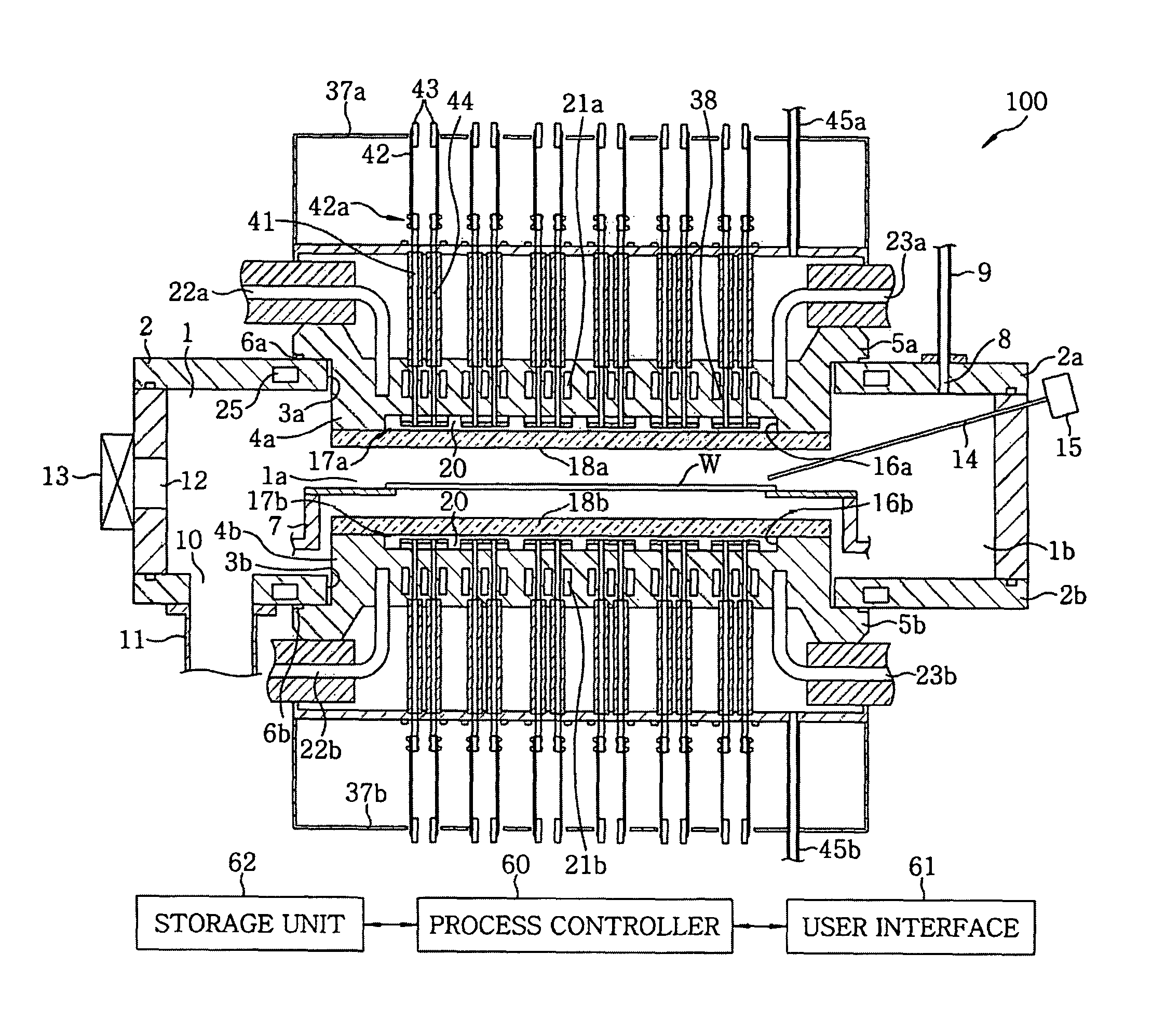
[0040]Hereinafter, embodiments of the invention will be described with reference to the accompanying drawings. An annealing apparatus for annealing a wafer of which surface is implanted with impurities will be described herein by way of example.

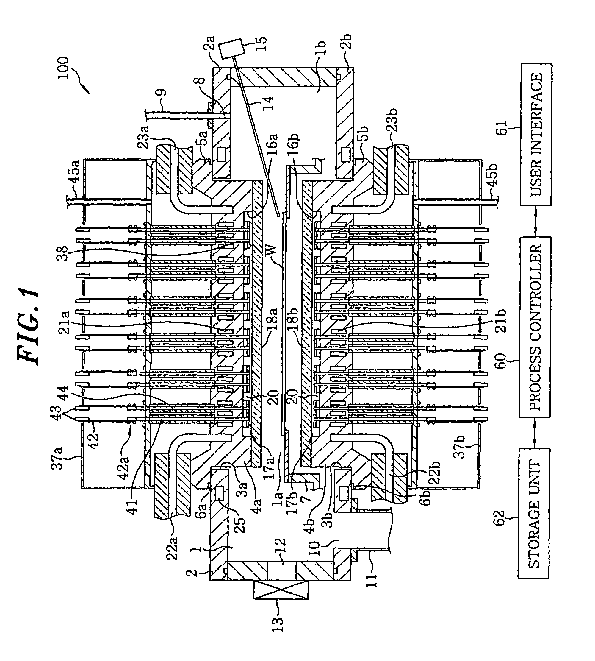
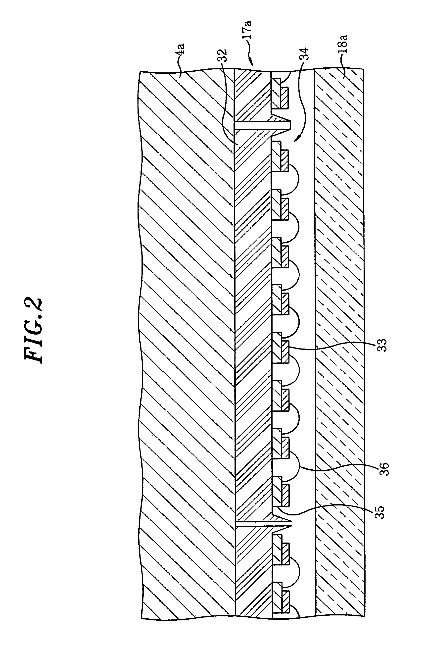
[0041]FIG. 1 is a sectional view showing a schematic configuration of an annealing apparatus in accordance with the embodiment of the present invention. FIG. 2 is an enlarged sectional view illustrating a heating source of the annealing apparatus shown in FIG. 1. FIG. 3 is an enlarged sectional view illustrating the portion through which to supply a power to LEDs of the annealing apparatus shown in FIG. 1. The annealing apparatus 100 includes an airtightly sealed processing chamber 1 into which a wafer W is loaded.

[0042]The processing chamber 1 has a cylindrical annealing portion 1a in which the wafer W is positioned and a gas diffusing portion 1b formed in a doughnut shape outside the annealing portion 1a. The gas diffusing portion 1b is gre...


PUM

PropertyMeasurementUnit
infrared ray wavelengthaaaaaaaaaa
pressureaaaaaaaaaa
temperatureaaaaaaaaaa

Abstract

Provided is an annealing apparatus, which is free from a problem of reduced light energy efficiency resulted by the reduction of light emission amount due to a heat generation and capable of maintaining stable performance. The apparatus includes: a processing chamber 1 for accommodating a wafer W; heating sources 17a and 17b including LEDs 33 and facing the surface of the wafer W to irradiate light on the wafer W; light-transmitting members 18a and 18b arranged in alignment with the heating sources 17a and 17b to transmit the light emitted from the LEDs 33; cooling members 4a and 4b supporting the light-transmitting members 18a and 18b at opposite side to the processing chamber 1 to make direct contact with the heating sources 17a and 17b and made of a material of high thermal conductivity; and a cooling mechanism for cooling the cooling members 4a and 4b with a coolant.

Description

FIELD OF THE INVENTION[0001]The present invention relates to an annealing apparatus for annealing a semiconductor wafer and the like by irradiating thereto lights emitted from light emitting devices such as LEDs or the like.BACKGROUND OF THE INVENTION[0002]In a manufacturing process of a semiconductor device, a semiconductor wafer (hereinafter simply referred to as “wafer”) as a substrate to be processed is subjected to film formation, oxidative diffusion, modification and various kinds of heat treatments such as annealing and the like. To meet high-speed and high-integration requirements in the semiconductor devices, the annealing performed after ion implantation requires high-speed heating and cooling for the purpose of minimizing diffusion. As an annealing apparatus capable of performing the high-speed heating and cooling, there has been proposed an annealing apparatus that employs LEDs (Light-Emitting Diodes) as a heating source (see, e.g., Patent Document 1).[0003]In case the L...

Claims


Application Information

Patent Timeline
Patent Type & Authority Patents(United States)
IPC IPC(8): H01L21/26C21D1/74
CPCH01L21/67109H01L21/67115H01L31/1864Y02E10/50Y02P70/50H01L21/26H01L21/324
Inventor KASAI, SHIGERUMIYASHITA, HIROYUKIYONEDA, MASATAKESUZUKI, TOMOHIROTANAKA, SUMINOMURA, MASAMICHISHIMIZU, MIWA
Owner TOKYO ELECTRON LTD
Why Eureka
Try Eureka