Spintronic device and information transmitting method

a technology of information transmission and spintronic device, which is applied in the direction of digital storage, instruments, galvano-magnetic material selection, etc., can solve the problems of joule heat and higher power consumption

Active Publication Date: 2012-08-28
NEC CORP
View PDF8 Cites 5 Cited by
  • Summary
  • Abstract
  • Description
  • Claims
  • Application Information

AI Technical Summary

Benefits of technology

[0029]The proposed spintronic device makes low-loss spin current transmission and transmission of an electric current via a magnetic dielectric material possible.

Problems solved by technology

Currently information transmission in information processing apparatuses is carried out using electron flow, which causes Joule heat.
Joule heat is a problem, in that the more the information processing unit is integrated, the higher the power consumption is, and therefore information transmission using spin current instead of electron flow has been investigated.

Method used


Image

  • Spintronic device and information transmitting method
  • Spintronic device and information transmitting method
  • Spintronic device and information transmitting method

Examples


first embodiment

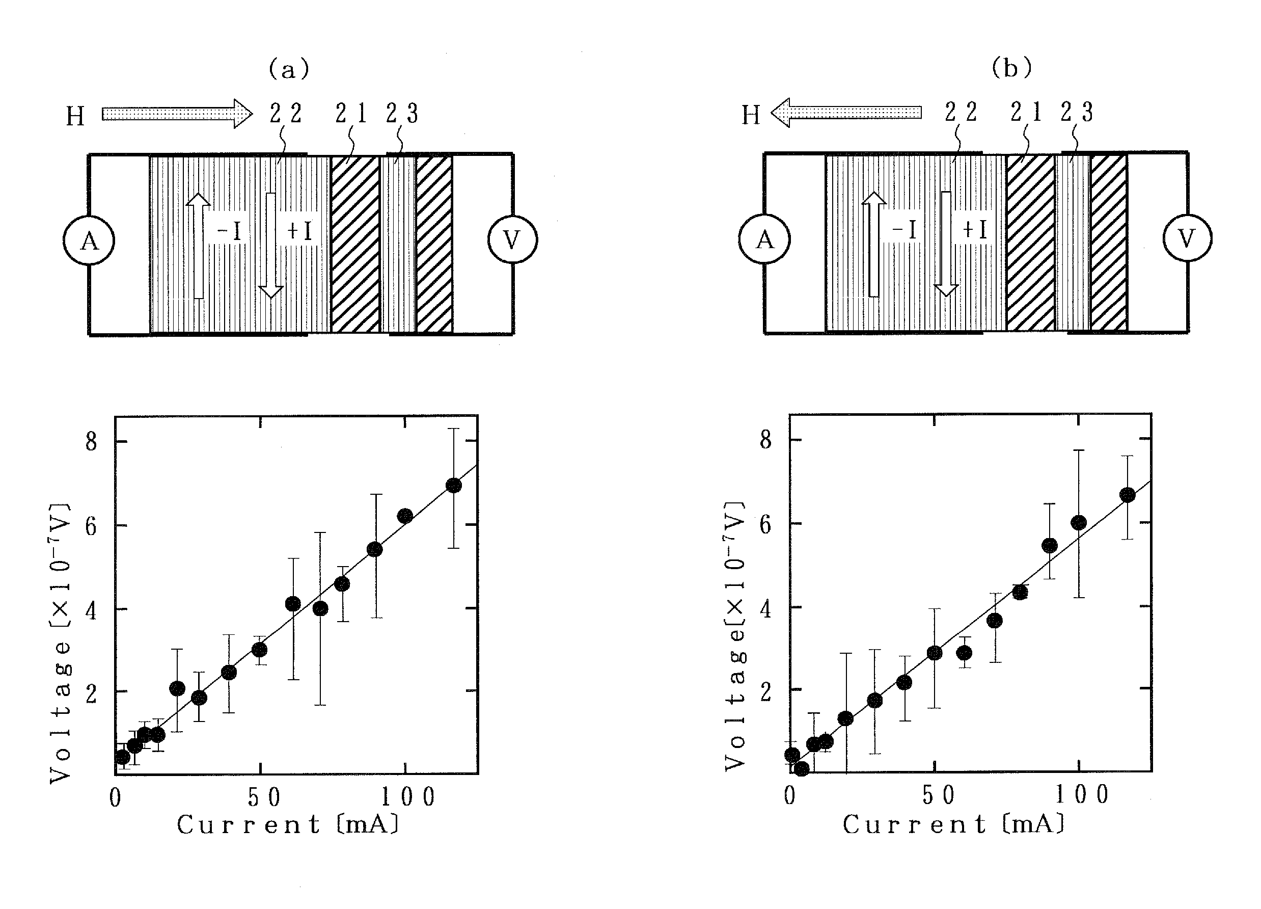
[0076]Next, the spintronic device according to the first embodiment of the present invention is described in reference to FIGS. 12(a) and 12(b). FIG. 12a is a conceptual diagram showing the structure of the spintronic device according to the first embodiment of the present invention, where a YIG layer 32 having a thickness of 50 nm and a Y3Fe4GaO12 composition is formed on a GGG single crystal substrate 31 in accordance with a sputtering method, and a Pt film having a thickness of 10 nm was deposited on top in accordance with a mask sputtering method, so that Pt electrodes 33 and 34 having a width of 1.0 mm were formed with a space of 5.0 mm in between.

[0077]FIG. 12(b) is a diagram illustrating an information transmitting method using a spintronic device where a pulse signal is applied to the Pt electrode 33 so that a pulse current flows through the Pt electrode and a pure pulse spin current is generated in a direction perpendicular to the direction of the pulse current due to the s...

second embodiment

[0081]Next, the spintronic device according to the second embodiment of the present invention is described in reference to FIG. 13. FIG. 13 is a conceptual diagram showing the structure of the spintronic device according to the second embodiment of the present invention, where an antiferromagnetic PdPtMn layer 35 having a thickness of 100 nm is deposited on top of a GGG single crystal substrate 31 in accordance with a sputtering method. A magnetic field is applied to the sample in the direction of the width when the antiferromagnetic PdPtMn layer 35 is deposited.

[0082]Next, a YIG layer 32 having a thickness of 50 nm and a Y3Fe4GaO12 composition is formed on top of the antiferromagnetic PdPtMn layer 35 in accordance with a sputtering method, and a Pt film having a thickness of 10 nm is deposited on top in accordance with a mask sputtering method, so that Pt electrodes 33 and 34 having a width of 1.0 mm are formed with a space of 5.0 mm in between.

[0083]In this case, all of the grains...


PUM


Abstract

A concrete means for making transmission over long distances possible using a spin-wave spin current is provided in a spintronic device and an information transmitting method.At least one metal electrode made of any of Pt, Au, Pd, Ag, Bi, alloys of these, or elements having an f-orbital are provided on top of a magnetic dielectric layer and, so that spin-wave spin current—pure spin current exchange is carried out at the interface between the above described magnetic dielectric layer and the above described metal electrode.

Description

TECHNICAL FIELD[0001]The present invention relates to a spintronic device and information transmitting method, and in particular to a spintronic device having a magnetic dielectric layer for transmitting a spin flow as a spin-wave spin current so that it can be transmitted over a distance of millimeters.BACKGROUND ART[0002]Currently in the field of electronics, for example with semiconductor devices, charge degree of freedom of electrons are used; electrons have spin degrees of freedom, in addition to charge degree of freedom. In recent years, spintronics using spin degree of freedom have been drawing attention as a next-generation carrier for information technology.[0003]In spintronics, the charge degree of freedom and the spin degree of freedom of electrons are simultaneously used in order to gain new functions and properties.[0004]Spin RAMs that control the direction of magnetization of a free layer using the spin of electrons which are carriers of a current by making a current f...

Claims


Application Information

Patent Timeline
Patent Type & Authority Patents(United States)
IPC IPC(8): G11C11/18
CPCG11C11/16H01F10/24H01L43/10G11C11/18G11C11/161G11C11/1675H10N50/85
Inventor KAJIWARA, YOSUKEUCHIDA, KENICHIANDO, KAZUYASAITOH, EIJI
Owner NEC CORP
Why Eureka
Try Eureka