Fabrication method of a non-planar transistor

a technology of non-planar transistors and fabrication methods, which is applied in the manufacturing of semiconductor/solid-state devices, basic electric elements, electric devices, etc., can solve the problems that current planar transistors no longer meet the requirements of products, and achieve the effect of enhancing the quality of non-planar transistors and facilitating diffusion into the fin regions

Active Publication Date: 2012-10-02
UNITED MICROELECTRONICS CORP
View PDF34 Cites 25 Cited by
  • Summary
  • Abstract
  • Description
  • Claims
  • Application Information

AI Technical Summary

Benefits of technology

[0006]The present invention therefore provides a fabrication method of a non-planar transistor, which can obtain a non-planar transistor having a fin structure with an anti-punch through doping region. Consequently, the quality of the devices can be improved.
[0008]Since the bottom doping regions are formed directly in the silicon substrate in the isolation regions, the dopant in the bottom doping regions can diffuse into the fin regions more easily during the annealing process. The anti-punch-through doping regions can therefore be formed in the fin structures, avoiding the problem of leakage current and enhancing the quality of the non-planar transistors.

Problems solved by technology

However, with the increasing miniaturization of electronic products, current planar FETs no longer meet the requirements of the products.

Method used


Image

  • Fabrication method of a non-planar transistor
  • Fabrication method of a non-planar transistor
  • Fabrication method of a non-planar transistor

Examples


first embodiment

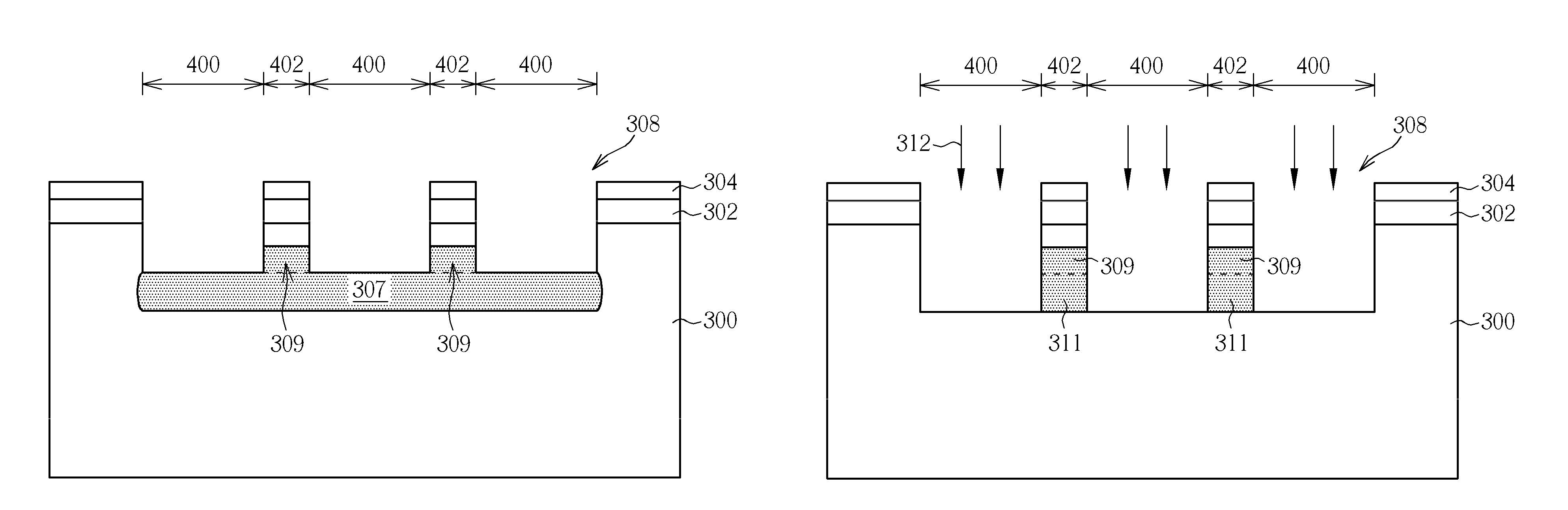
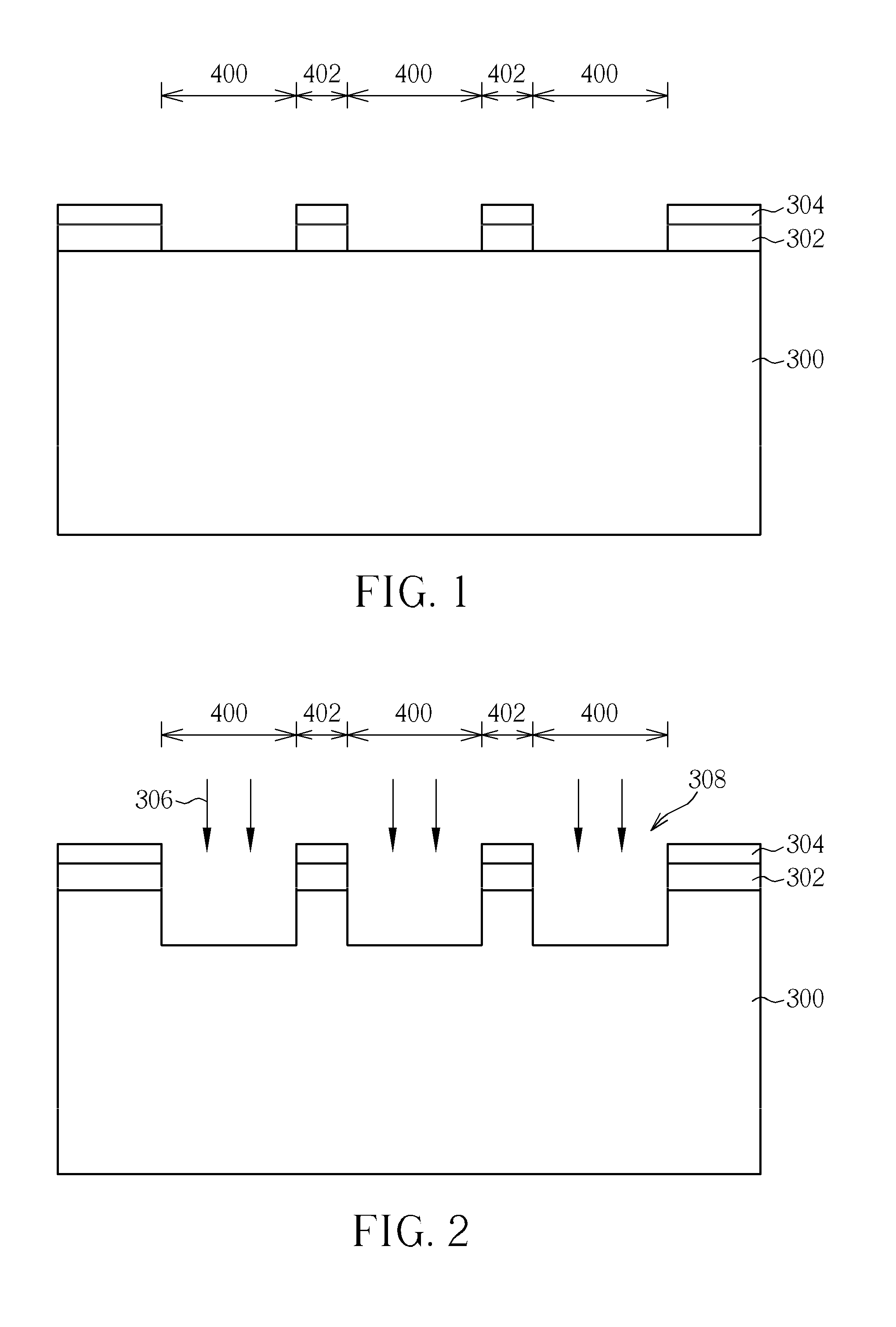
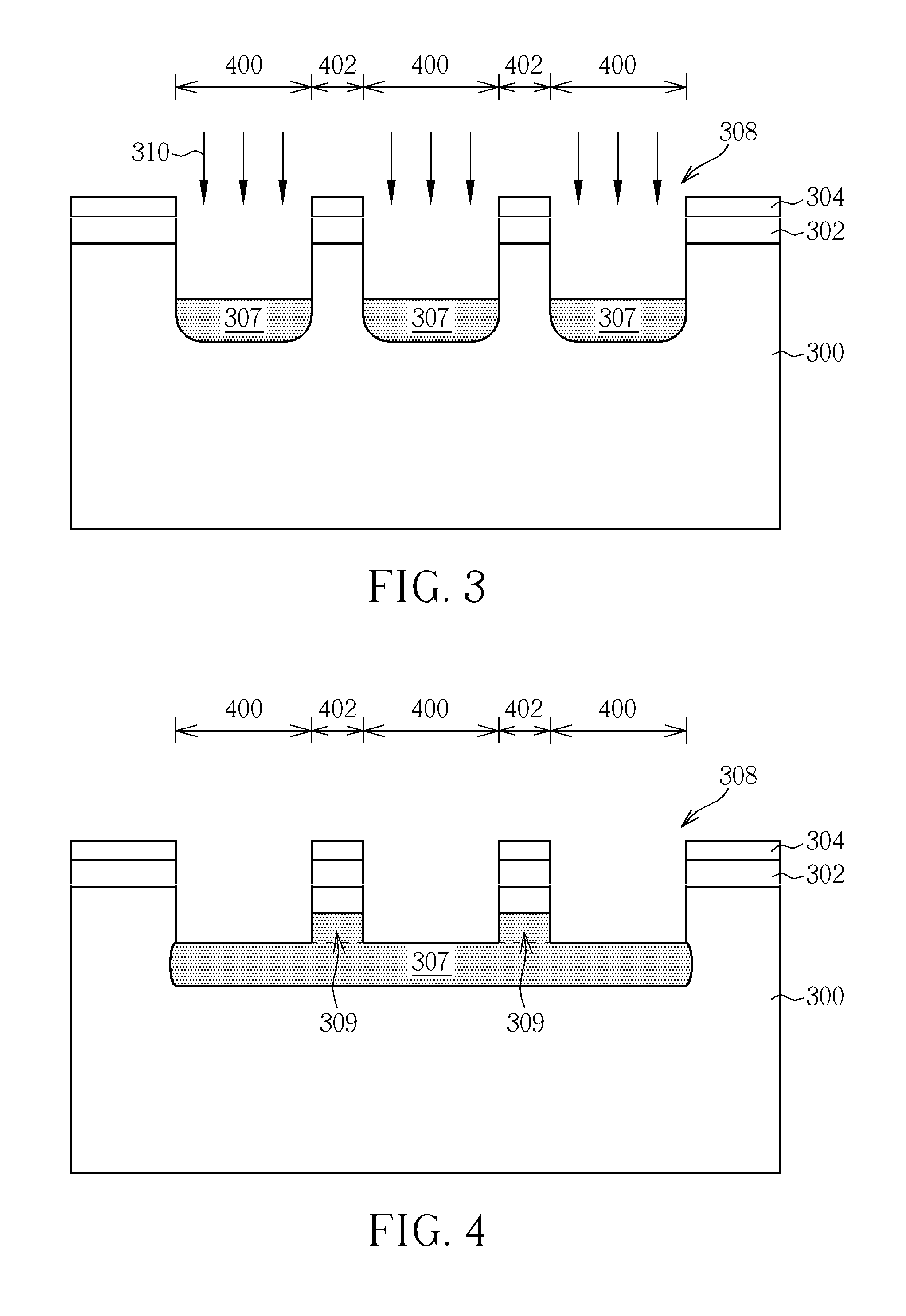
[0013]Please refer to FIG. 1 to FIG. 9, illustrating schematic diagrams of the fabrication method of a non-planar FET in the present invention. As shown in FIG. 1, a substrate 300, an optional pad layer 302 and a mask layer 304 are provided. By using a lithography process and an etching process, the pad layer 302 and the mask layer 304 are patterned, thereby defining a plurality of isolation regions 400 and a plurality of fin regions 402. Each isolation region 400 and each fin regions 402 are arranged alternatively with each other. In the subsequent steps, a shallow trench isolation will be formed in the isolation region 400 and a fin structure of a non-planar transistor will be formed in the fin region 402. The patterned pad layer 302 and the patterned mask layer 304 expose the substrate 300 in the isolation regions 400. In one embodiment, the substrate 300 may include a silicon substrate, an epitaxial silicon substrate, a silicon germanium substrate, a silicon carbide substrate o...

second embodiment

[0021]Please refer to FIG. 10, illustrating a schematic diagram of the fabrication method of a non-planar FET in the present invention. As shown in FIG. 10, before performing the second etching process, a trimming process can be performed toward the patterned pad layer 302 and the patterned mask layer 304 to reduce the areas thereof. Thus, when performing the second etching process 312 by using the lessened patterned pad layer 302 and the patterned mask layer 304 as a mask, the fin structure 311 forms a curved corner between the top surface and the sidewall. Consequently, an uneven electrical field in the corner of the fin structure 311 can be avoided. In another embodiment, the trimming process can be performed after the second etching process.

[0022]In summary, the present invention provides a fabrication method of a non-planar transistor, which can obtain a non-planar transistor having a fin structure with an anti-punch-through doping region. Since the bottom doping regions are f...


PUM


Abstract

A method of forming a non-planar transistor is provided. A substrate is provided. The substrate has a plurality of isolation regions to be formed and a plurality of fin regions to be formed. A first etching process is performed to form a plurality of first trenches having a first depth in the substrate within the isolation regions. At least a doping region is formed in the substrate within the fin regions. A second etching process is performed to deepen the first depth to a second depth and a plurality of fin structures are formed in the substrate within the fin regions. Lastly, a gate is formed on the fin structures.

Description

BACKGROUND OF THE INVENTION[0001]1. Field of the Invention[0002]The present invention relates to a fabrication method of a non-planar transistor, and more particularly, to a fabrication method of a non-planar transistor having a fin structure with an anti-punch-through doping region.[0003]2. Description of the Prior Art[0004]In recent years, as various kinds of consumer electronic products are being constantly modified towards increased miniaturization, the size of semiconductor components are modified to be reduced accordingly, in order to meet high integration, high performance, low power consumption, and the demands of products.[0005]However, with the increasing miniaturization of electronic products, current planar FETs no longer meet the requirements of the products. Thus, non-planar FETs such as Fin-shaped FETs (Fin-FET) have been developed, which includes a three-dimensional channel structure. The manufacturing processes of Fin-FET devices can be integrated into traditional l...

Claims


Application Information

Patent Timeline
Patent Type & Authority Patents(United States)
IPC IPC(8): H01L21/76
CPCH01L21/823431H01L21/76224H01L21/324
Inventor CHEN, YING-TSUNGLIN, CHIEN-TINGTSAI, SHIH-HUNGFU, SSU-ICHIANG, WEN-TAI
Owner UNITED MICROELECTRONICS CORP
Why Eureka
Try Eureka