Plane emission device

a technology of emission device and emission chamber, which is applied in the direction of discharge tube luminescnet screen, semiconductor/solid-state device details, transportation and packaging, etc., can solve the problems of reducing the luminous efficiency of the organic el device, and achieve the effect of increasing the incident efficiency of lights to the transparent substrate and increasing the takeout efficiency of lights to the outsid

Active Publication Date: 2012-10-09
SAMSUNG DISPLAY CO LTD
View PDF28 Cites 13 Cited by
  • Summary
  • Abstract
  • Description
  • Claims
  • Application Information

AI Technical Summary

Benefits of technology

[0011]The present invention is conceived in view of the problems mentioned above, and purposed to provide a plane emission device which enables to improve the takeout efficiency of lights by restricting the total reflection of lights on the boundary face of the transparent electrode layer and the alleviation layer.
[0013]According to such a configuration, since the light scattering layer formed between the transparent substrate and the luminescent body layer is formed to contain the binder and the two kinds of fillers satisfying the above mentioned relationship of the refraction indexes, light scattering effect is magnified, disorder occurs in critical angles when lights emitted in the luminescent body layer exit from the light scattering layer to the transparent substrate, incident efficiency of lights to the transparent substrate is increased, and takeout efficiency of lights to outside becomes much larger.

Problems solved by technology

However, even if the quantum efficiency is drastically improved as above, when the takeout efficiency of lights is lower, it causes to decrease the luminous efficiency of the organic EL device due to the fact.

Method used


Image

  • Plane emission device
  • Plane emission device
  • Plane emission device

Examples


first embodiment

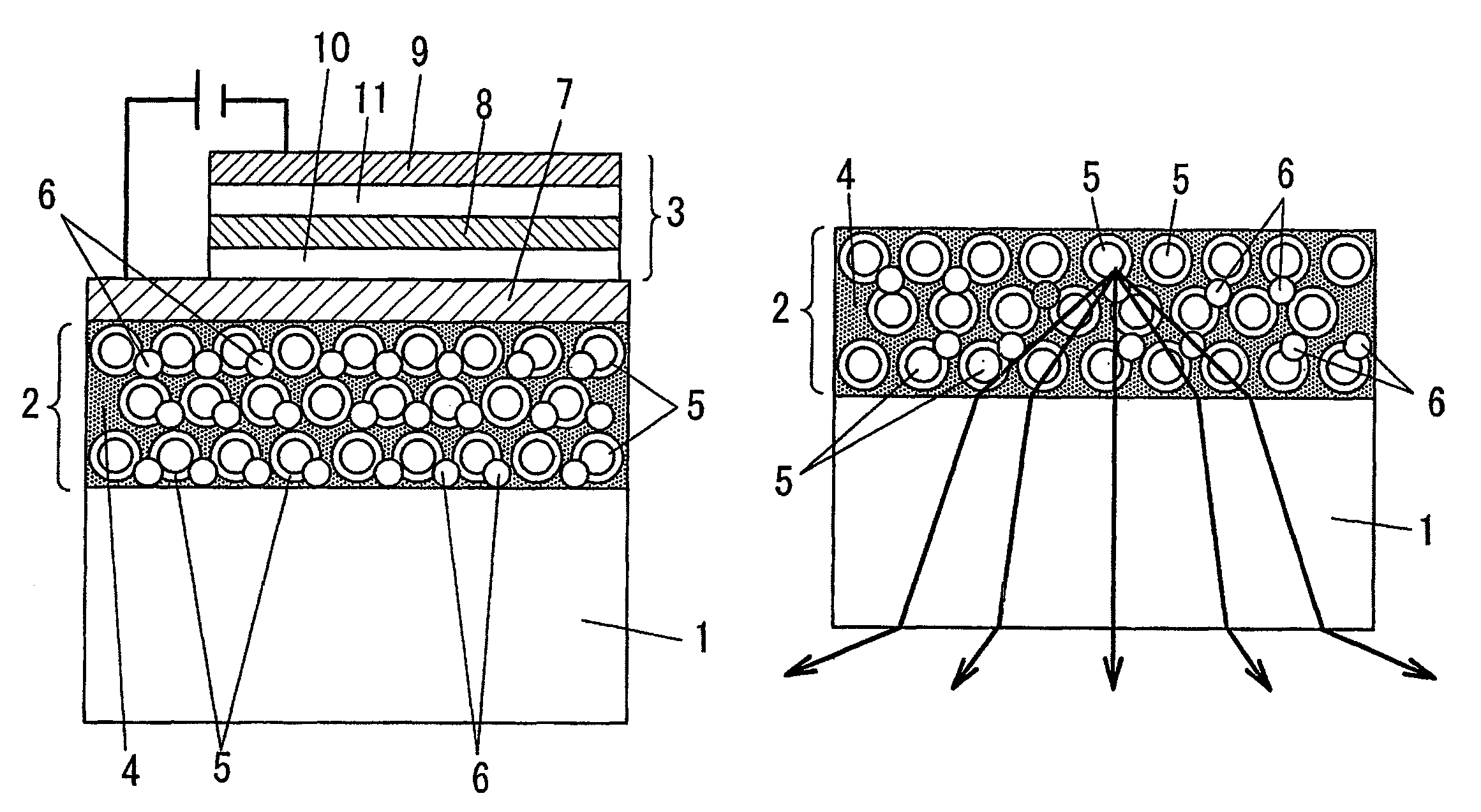
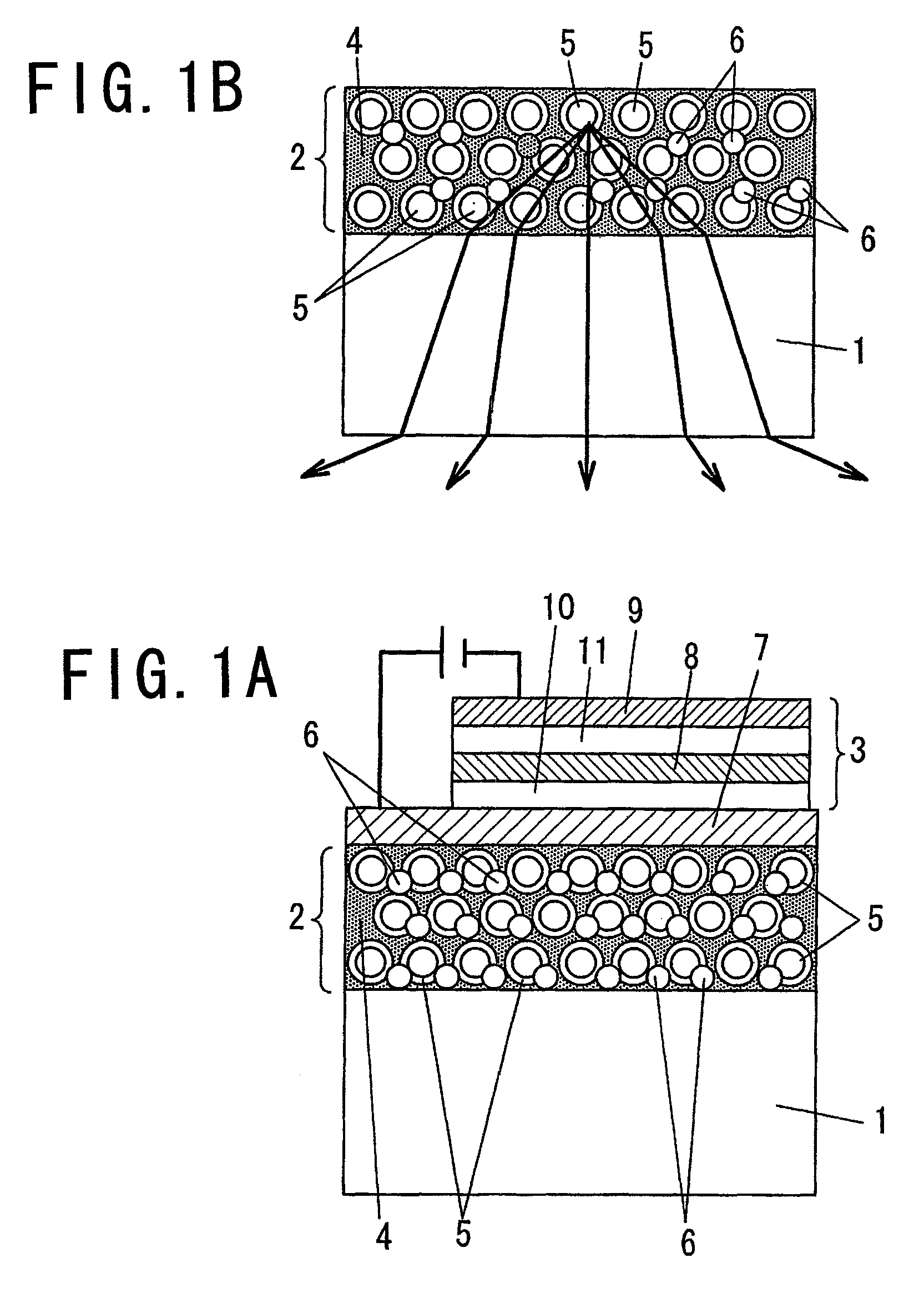
[0017]A plane emission device in accordance with a first embodiment of the present invention is described with reference to FIG. 1A and FIG. 1B. FIG. 1A shows a configuration of a plane emission device in accordance with the first embodiment, and FIG. 1B shows a configuration of a light scattering layer 2 formed on a surface of a transparent substrate 1.

[0018]As for a luminescent body 3, an organic or an inorganic one which emits lights by light or electric energy can be used. The luminescent body 3 shown in FIG. 1A is one which emits lights owing to be activated by electric energy, such as an organic EL device. The luminescent body 3 is configured of a transparent electrode layer (anode) 7 which is formed on the light scattering layer 2, a luminescent layer 8, an opposing electrode (cathode) 9 and a hole transfer layer 10 and an electron transfer layer 11 which are provided according to need, and so on. Lights emitted in the luminescent layer 8 pass through the transparent electrod...

example 1

Practical Example 1

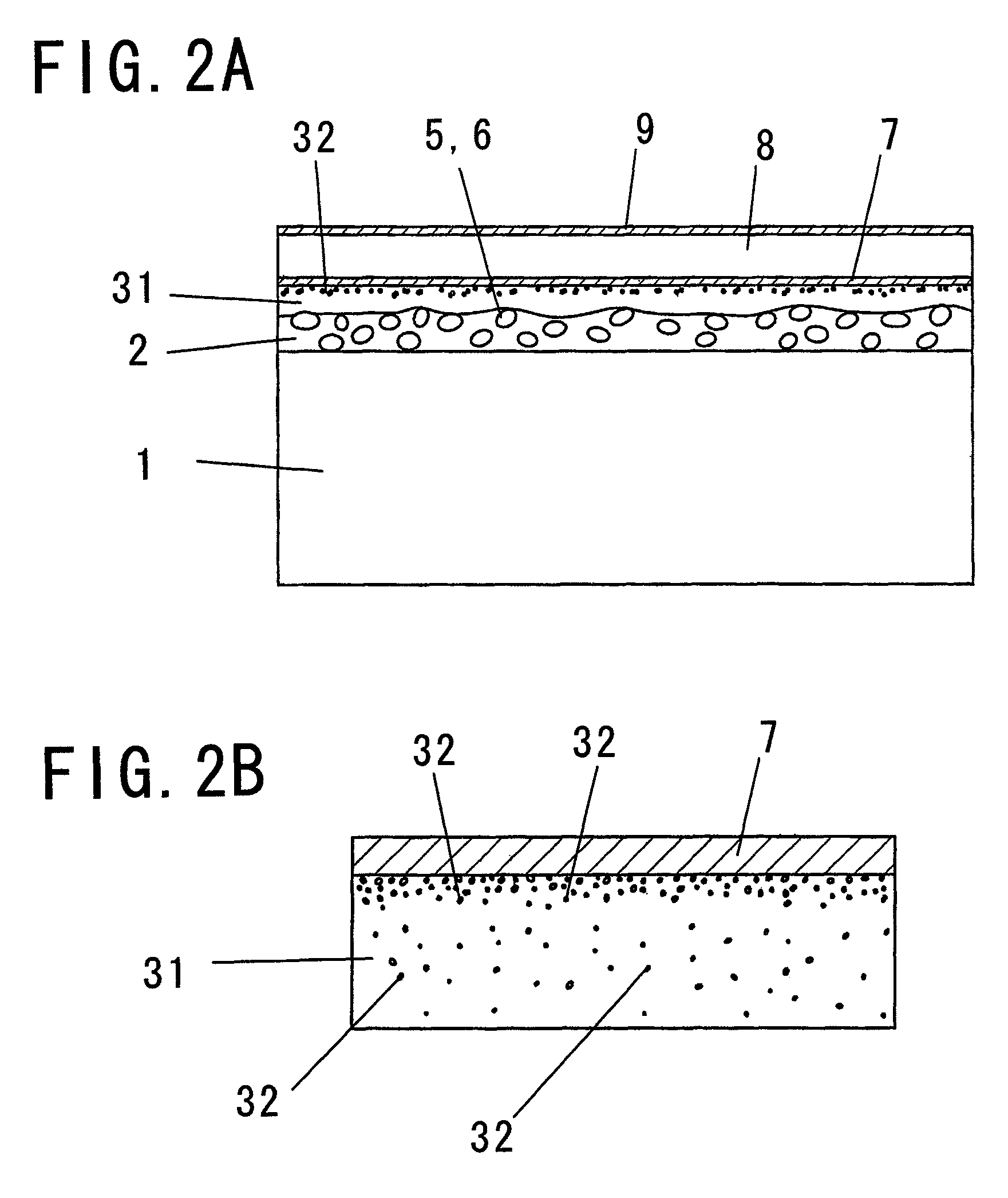
[0042]A solution was obtained by adding 803.5 masses part of isopropyl alcohol into 86.8 masses part of tetraethoxysilane, and further adding 34.7 mass part of γ-methacryloxypropyltrymethoxysilane and 75 mass part of 0.1N-nitric acid, and mixing it well with by dispersion mill. The obtained solution was agitated two hours in thermostatic oven at 40 degrees Celsius, and thus, 5 weight % of silicone resin solution was obtained as a binder silicone resin having 1050 weight average molecular weight.

[0043]Subsequently, a silicone resin solution containing hollow silica fine particles was obtained by adding a sol that an IPA dispersed sol (solid content: 20 mass %, dispersion medium: isopropyl alcohol, made by Catalysts and Chemicals Ltd.) of hollow silica fine particles (mean particle diameter: 60 nm, outer shell thickness: 10 nm) was diluted by isopropyl alcohol to be 5 mass % into the silicone resin solution so that hollow silica fine particles / silicone resin (conden...

example 2

Practical Example 2

[0052]In order to make the refraction index of the light scattering layer 2 smaller than the refraction index of the transparent substrate 1, a coating materials composition was prepared by adding hollow silica fine particles / silica-titania compound fine particles / silicone resin (condensation chemical compound conversion) into silicone resin solution obtained in the above mentioned practical example 1 so as to be 60 / 10 / 30 on the basis of solid content mass standard, and a light scattering layer 2 was formed with this coating materials composition similar to the practical example 1. The refraction index of the light scattering layer 2 was 1.39 which was smaller than the refraction index 1.51 of the transparent substrate 1. Then, an organic EL device (luminescent body) 3 was formed on the light scattering layer 2 similar to the practical example 1, and thus, a plane emission device was obtained.


PUM


Abstract

In a plane emission device comprising a transparent substrate, a light scattering layer formed on a surface of the transparent substrate, and a luminescent body of organic or inorganic material which is formed on a surface of the light scattering layer and emits light by light or electric energy, efficiency to takeout light to outside is improved. The light scattering layer contains binder and two kinds of fillers, and when a refraction index of the binder is assumed as Nb, a refraction index of one of the two kinds of fillers is assumed as Nf1, and a refraction index of the other is assumed as Nf2, a relationship that Nf2>Nb>Nf1 is satisfied. Since the light scattering layer contains two kinds of fillers, disorder occurs in critical angle when light exits from the light scattering layer to the transparent substrate, incidence rate of light into the transparent substrate rises, and efficiency to takeout the light to outside increases.

Description

TECHNICAL FIELD[0001]The present invention relates to a plane emission device which is used in various kinds of display units, a display device, a back light for a liquid crystal display, or a light source of a lighting system.BACKGROUND ART[0002]A plane emission device emitting lights by light or electric energy, which is used for a light source of various kinds of display units, a display device, a back light, or a lighting system, has many superior characteristics such as high-luminance, high-efficiency, low-profile and light-weight. Among the plane emission devices, an organic electroluminescence device (organic EL device), which makes organic materials emit lights by electric energy from an anode and a cathode, is energetically researched and developed for practical use, because it enables high-luminance plane emission with a low voltage about several Volt, and enables the light emission with arbitrary color tone by selection of luminescent materials.[0003]The organic EL device...

Claims


Application Information

Patent Timeline
Patent Type & Authority Patents(United States)
IPC IPC(8): H01J5/16
CPCB82Y20/00B82Y30/00H01L51/5268Y10T428/24942H01L2251/5369Y02E10/549H10K50/854H10K2102/331H01L23/295H10K30/82
Inventor ITOU, NORIHIROYAMAKI, TAKEYUKIIDE, NOBUHIROKAWANO, KENJI
Owner SAMSUNG DISPLAY CO LTD
Why Eureka
Try Eureka