Nonvolatile SRAM/latch circuit using current-induced magnetization reversal MTJ

a current-induced magnetization reversal, non-volatile technology, applied in the field of memory circuits, latch circuits, flipflop circuits, can solve the problems of volatile d latch circuits consuming power while, data stored in bistable circuits b>30/b> is lost, and sram consumes power, etc., to achieve high speed

Active Publication Date: 2012-10-23
JAPAN SCI & TECH CORP
View PDF7 Cites 25 Cited by
  • Summary
  • Abstract
  • Description
  • Claims
  • Application Information

AI Technical Summary

Benefits of technology

[0046]According to the present invention, it is possible to write data in and read out data from the bistable circuit at high speed. In addition, even though a power source is shut down, it is possible to restore data nonvolatilely stored in a ferromagnetic tunnel junction device to the bistable circuit. Therefore, it becomes possible to read out data stored before a power source is shut down even though the power source is restored after the power source is shut down.

Problems solved by technology

However, an SRAM consumes power while holding data.
In addition, when the power source is shut down, data stored in the bistable circuit 30 is lost.
A volatile D latch circuit consumes power while holding data.
In addition, if the power source is shut down, the data stored in the bistable circuit 30 is lost.

Method used


Image

  • Nonvolatile SRAM/latch circuit using current-induced magnetization reversal MTJ
  • Nonvolatile SRAM/latch circuit using current-induced magnetization reversal MTJ
  • Nonvolatile SRAM/latch circuit using current-induced magnetization reversal MTJ

Examples


sixth embodiment

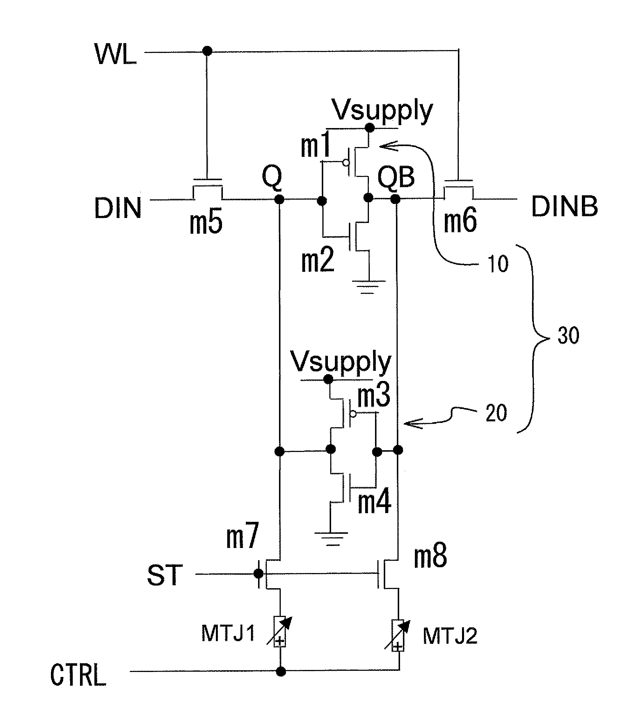
[0150]FIG. 23A and FIG. 23B are circuit diagrams of a memory circuit in accordance with the sixth embodiment. In the sixth embodiment, compared to the fifth embodiment, a resistance R1 contacts with a ground. Since data in the bistable circuit 30 is stored to the ferromagnetic tunnel junction device MTJ1, it is not necessary for the current to flow in the resistance R1 when the control line CTRL is high level. Therefore, a resistance R1 can contact with a ground. As same with the fifth embodiment, the resistance R1 is set to be between a high resistance Rap and a low resistance Rp. In addition, the FET m7 and the FET m8 can be provided as illustrated in FIG. 23A, and do not have to be provided as illustrated in FIG. 23B.

seventh embodiment

[0151]FIG. 24 is a circuit diagram of a memory circuit in accordance with the seventh embodiment. In the seventh embodiment, an output of an amplifier circuit 70 including a two-stage inverter composed of FETs m9 through m12 is coupled to the control line CTRL in FIG. 5 of the second embodiment. An external control line EXT-CTRL is coupled to an input of the amplifier circuit 70, If many memory circuits are controlled with the control line CTRL at the same time, operations will get slow. According to the seventh embodiment, the store and restoration in the memory circuit can be performed at high speed because a signal of the external control line EXT-CTRL is amplified by the amplifier circuit 70.

eighth embodiment

[0152]FIG. 25 is a circuit diagram of a memory circuit in accordance with the eighth embodiment. In the eighth embodiment, an n-type MOSFET m13 is coupled between the control line CTRL and a ground, and the gate of the FET m13 is coupled to the second control line RCL. FIG. 26 is a timing diagram of the memory circuit in accordance with the eighth embodiment. When storing, the level of the second control line RCL is at a low level. The FET m13 becomes non-conductive. Therefore, because one of nodes Q and QB has a high level potential and the other has a low level potential, the current flows between the ferromagnetic tunnel junction device MTJ1 and the ferromagnetic tunnel junction device MTJ2, and data in the bistable circuit 30 is stored to ferromagnetic tunnel junction devices MTJ1 and MTJ2. At this time, the voltage of the control line CTRL becomes interlevel between a high level and a low level. When restoring, the second control line RCL is at a high level. As the control line...


PUM


Abstract

The present invention is a memory circuit that includes a bistable circuit that stores data; and a ferromagnetic tunnel junction device that nonvolatilely stores the data stored in the bistable circuit according to a magnetization direction of a ferromagnetic electrode free layer, the data nonvolatilely stored in the ferromagnetic tunnel junction device being able to be restored in the bistable circuit. According to the present invention, writing data to and reading data from the bistable circuit can be performed at high speed. In addition, even though a power source is shut down, it is possible to restore data nonvolatilely stored in the ferromagnetic tunnel junction devices to the bistable circuit.

Description

TECHNICAL FIELD[0001]The present invention relates to a memory circuit, a latch circuit, and a flip-flop circuit, especially relates to a memory circuit, a latch circuit, and a flip-flop circuit including a bistable circuit and a ferromagnetic tunnel junction device.BACKGROUND ART[0002]An SRAM (Static Random Access Memory) has been well known as a volatile memory circuit used for an electronic apparatus. FIG. 1 is a circuit diagram illustrating a memory cell of an SRAM using MOS (Metal Oxide Semiconductor) Field Effect Transistor (FET). The memory cell has a bistable circuit 30, two input / output transistors m5 and m6. A CMOS inverter 10 (a first inverter circuit) and a CMOS inverter 20 (a second inverter circuit) are coupled in a ring shape in the bistable circuit 30. The inverter 10 includes a p-type MOSFET m1 and an n-type MOSFET m2. In the FET m1 and the FET m2, sources are coupled to a power source Vsupply and a ground respectively, gates are commonly-coupled to a node Q, and dr...

Claims


Application Information

Patent Timeline
Patent Type & Authority Patents(United States)
IPC IPC(8): G11C11/00
CPCG11C14/0081
Inventor YAMAMOTO, SHUICHIROSUGAHARA, SATOSHI
Owner JAPAN SCI & TECH CORP
Why Eureka
Try Eureka