

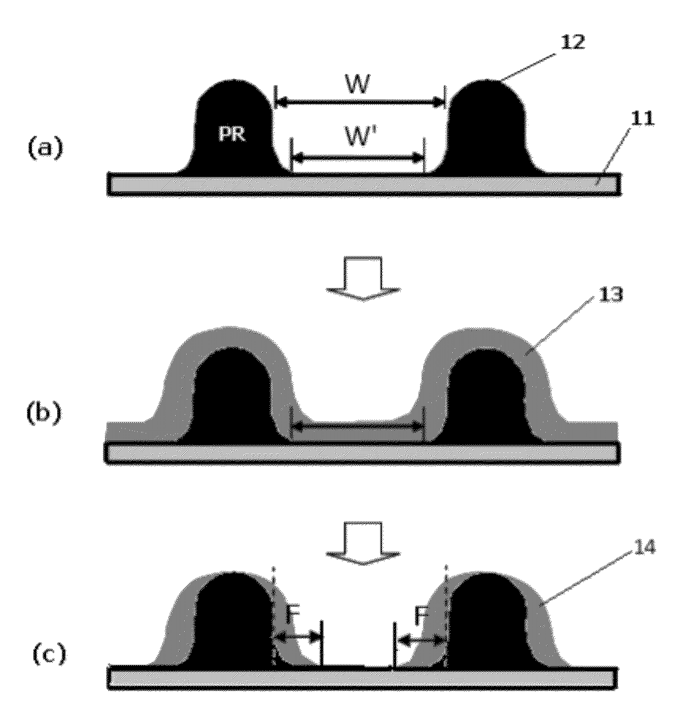
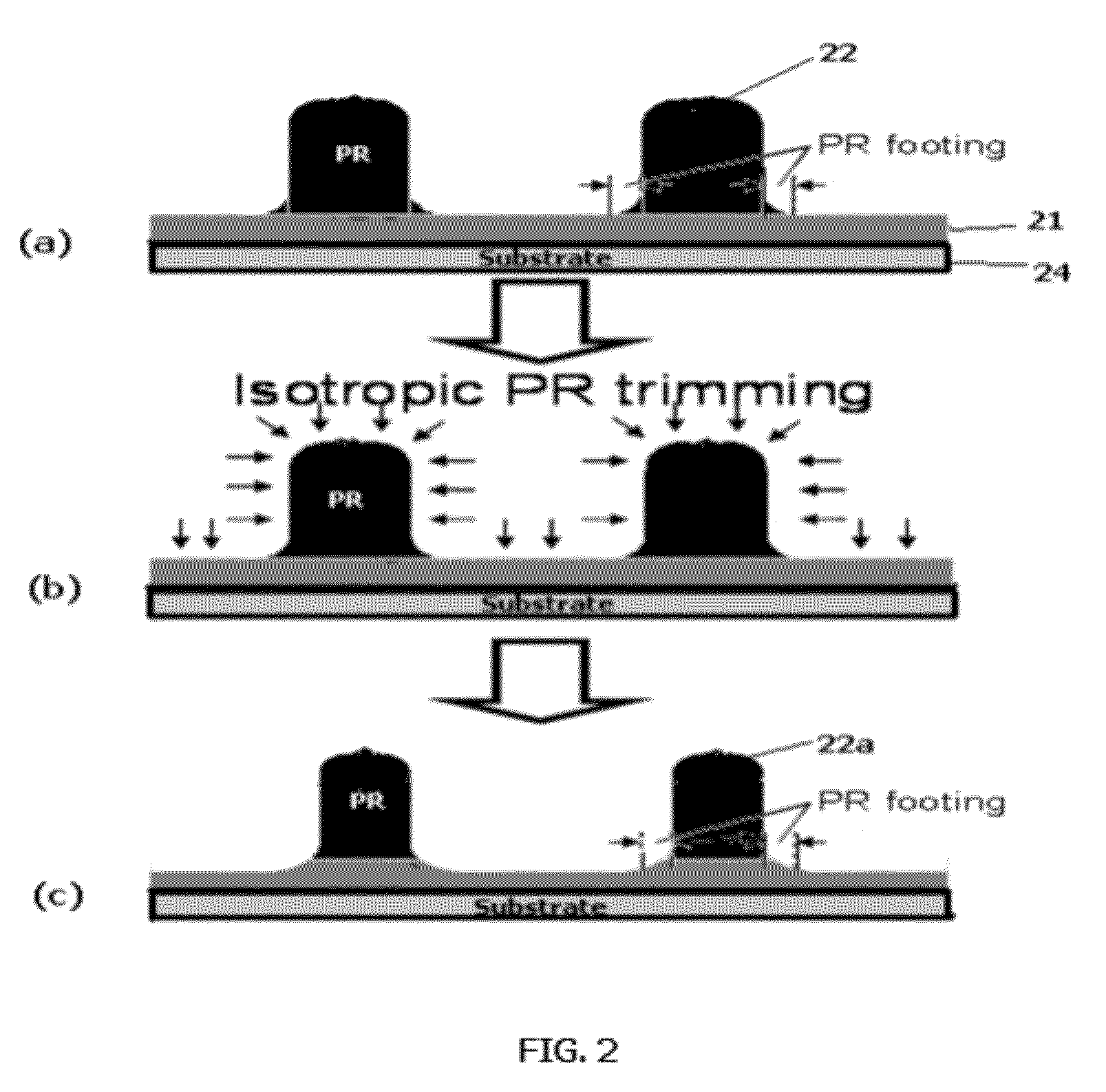
Footing reduction using etch-selective layer
a selective layer and footing technology, applied in the direction of decorative surface effects, electrical appliances, decorative arts, etc., can solve the problems of difficult control of the transfer footing shape, unexpected critical dimension (cd) changes or the like, and the difficulty of forming patterns with pitches, etc., to reduce the widened footing of the photoresist and the effect of reducing the etch ra
- Summary
- Abstract
- Description
- Claims
- Application Information
AI Technical Summary
Benefits of technology
Problems solved by technology
Method used
Image

Examples
Embodiment Construction
[0020]In this disclosure, “gas” may include vaporized solids and / or liquids and may be constituted by a mixture of gases. In this disclosure, the reactant gas, the additive / carrier gas, and the precursor may be different from each other or mutually exclusive in terms of gas types, i.e., there is no overlap of gases among these categories. In some embodiments, “film” refers to a layer continuously extending in a direction perpendicular to a thickness direction substantially without pinholes to cover an entire target or concerned surface, or simply a layer covering a target or concerned surface. In some embodiments, “layer” refers to a structure having a certain thickness formed on a surface or a synonym of film. In this disclosure, any defined meanings do not necessarily exclude ordinary and customary meanings in some embodiments. In the disclosure, “substantially lower”, “substantially higher”, “substantially different”, etc. refer to a difference of at least 10%, 50%, 100%, 200%, 3...
PUM
| Property | Measurement | Unit |
|---|---|---|
| heat resistance | aaaaa | aaaaa |
| heat resistance | aaaaa | aaaaa |
| width | aaaaa | aaaaa |
Abstract
Description
Claims
Application Information