Hermetic encapsulation of organic, electro-optical elements

a technology applied in the field of organic and electrooptical elements, can solve the problems of inability to extend the operating time of oleds to more than 5000 operating hours, limited service life, etc., and achieve the effect of reducing work function, effective protection against element degradation, and difference in work function

Active Publication Date: 2012-10-30
SCHOTT AG
View PDF25 Cites 4 Cited by
  • Summary
  • Abstract
  • Description
  • Claims
  • Application Information

AI Technical Summary

Benefits of technology

[0050]Furthermore, the process according to the invention can advantageously be improved if it additionally comprises the step of applying at least one bonding layer, in particular a bonding layer to which the at least one layer with a vitreous structure is applied. A layer of this type can in particular improve the bonding properties of the layer with a vitreous structure on plastic surfaces, which has advantageous effects on the mechanical stability of the layer microstructure under thermal or mechanical loads, for example a bending load. In this way, a continuous layer is produced more quickly and it is possible to achieve smoother layers with a lower porosity.
[0051]The invention also envisages the provision of an organic photoelectric element which is producible in particular by the process described above.
[0052]Accordingly, an element according to the invention comprises: a substrate, a first conductive layer, at least one layer which includes at least one organic, electro-optical material, and a second conductive layer, as well as a deposited layer with a vitreous structure.
[0053]As has already been described above in connection with the process for producing OLEDs, a layer with a vitreous structure is particularly suitable as a diffusion barrier for small molecules, and therefore provides effective protection against degradation of the element. The fact that the layer is deposited on a surface of the element means that there is a join between the layer and the surface without intermediate or transition layers, which is particularly expedient with a view to achieving a hermetic seal. The layer is preferably deposited on the surface by means of CVD and / or PVD, for example by sputtering, evaporation-coating, PCVD or PICVD.
[0054]It is preferable for one of the conductive layers to have a lower work function than the other conductive layer, in order to create a difference in work function between the layers. In the case of a light-emitting element, when a voltage is applied to the conductive layers electrons are injected from the layer with a lower work function into unoccupied energy states. Recombination with defect electrons which are injected from the layer with a higher work function then leads to light quanta being emitted.
[0055]To increase the quantum efficiency of an OLED according to the invention, the OLED may additionally have further functional layers. In this context, by way of example, at least one hole injection layer and / or at least one potential-matching layer and / or at least one electron blocker layer and / or at least one hole blocker layer and / or at least one electron conductor layer and / or hole conductor layer and / or at least one electron injection layer are advantageous.

Problems solved by technology

However, the main problem with OLEDs is their service life, which has hitherto been very limited.
It has proven almost impossible to extend the operating time of OLEDs to more than 5000 operating hours.
However, these materials with a low work function are generally highly reactive.
Chemical reactions undergone by the metal layer and associated changes in the work function are considered to be one of the main factors limiting the service life.
A drawback of this solution is that organic layers, such as the bonding area between metal sheet and glass substrate, are relatively easy for small gas molecules to penetrate.
Therefore, it is only a question of time until the drying agent is exhausted and degradation of the metal electrode commences.
Furthermore, this type of encapsulation makes it impossible to implement significant properties of the OLED technology, such as the encapsulation of extremely thin or flexible components.
However, a common feature of all these solutions which are known from the prior art is that the efficiency of the getter material falls as the incidence of gas continues, and consequently there is no permanent protection against degradation.

Method used


Image

  • Hermetic encapsulation of organic, electro-optical elements
  • Hermetic encapsulation of organic, electro-optical elements
  • Hermetic encapsulation of organic, electro-optical elements

Examples


Embodiment Construction

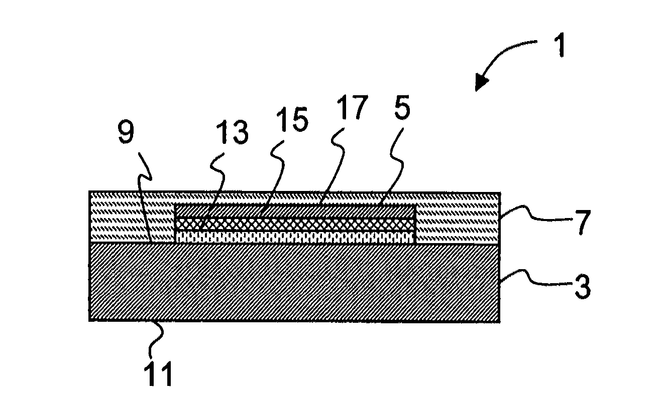
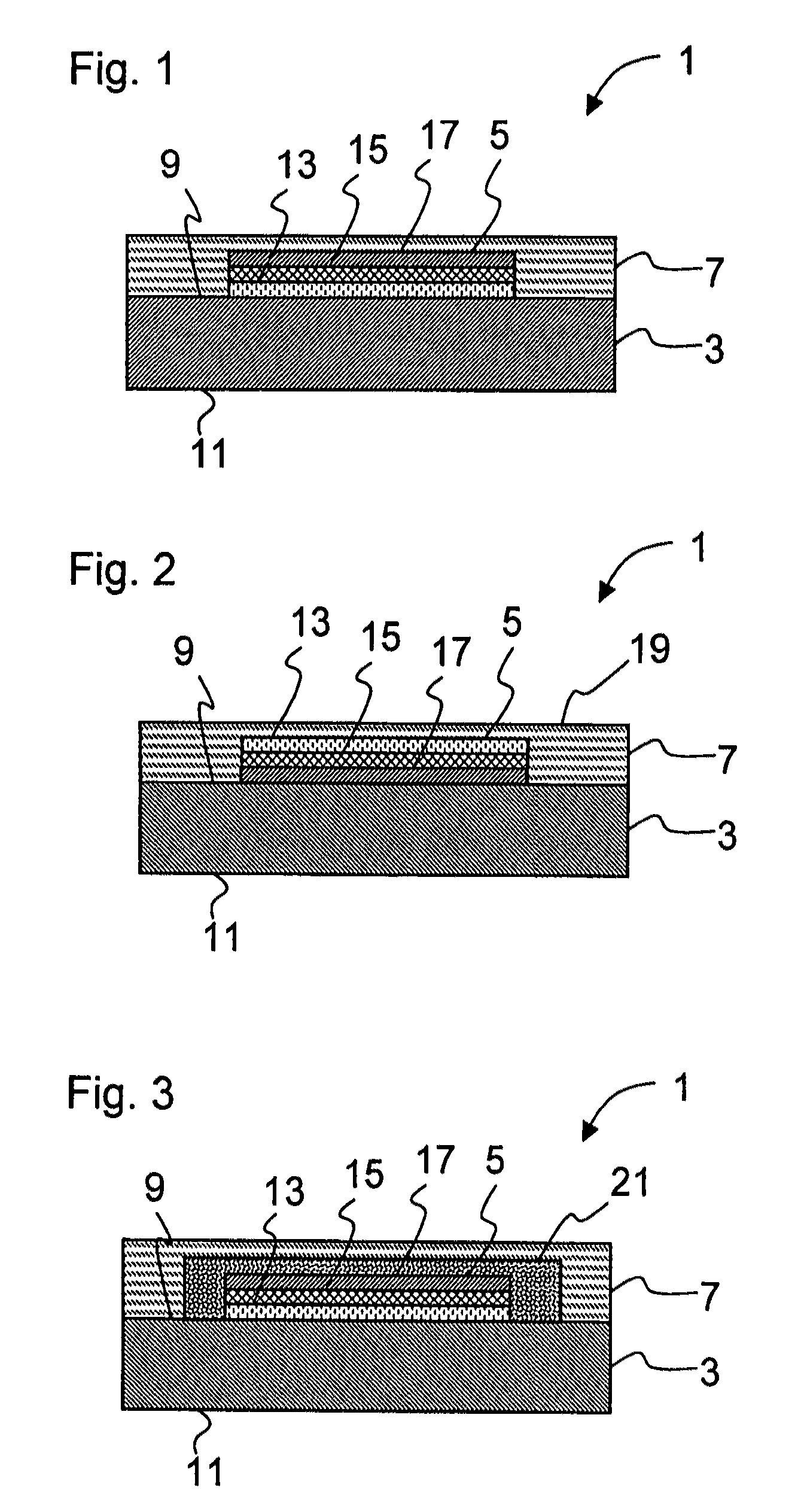
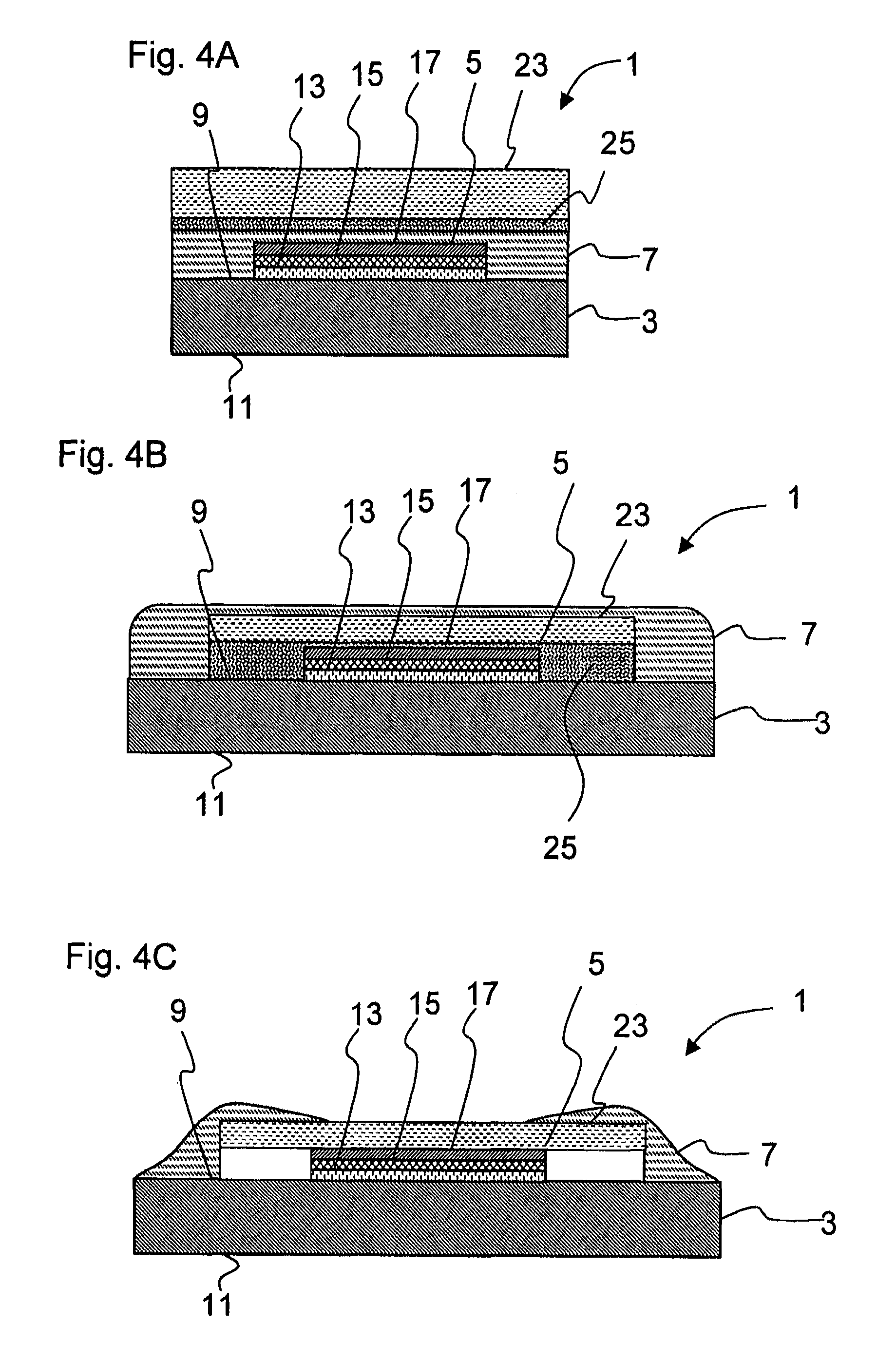
[0082]FIG. 1 shows a diagrammatic cross-sectional view through a first embodiment of an OLED according to the invention, which is denoted overall by 1. The OLED comprises a substrate 3, to which an OLED layer structure 5 is applied on one side 9. The layer structure 5 comprises a first conductive layer 13, a layer 15 which includes at least one organic, electro-optical material, and a second conductive layer 17. The layer structure 5 of the OLED is covered with a layer 7 with a vitreous structure and has been applied by means of PVD and / or CVD coating. On account of its low permeability, the layer 7 creates a hermetic encapsulation of the OLED layer structure 5, in particular with respect to small gas molecules from natural atmosphere, such as water or oxygen. In this way, the degradation of the OLED according to the invention as a result of chemical reactions between reactive gases and materials of the layer structure is greatly reduced, and this manifests itself in an increased se...


PUM

PropertyMeasurementUnit
thicknessesaaaaaaaaaa
thicknessaaaaaaaaaa
thicknessaaaaaaaaaa

Abstract

A process for producing increased service life of organic, electro-optical elements is provided. The process includes the steps of: providing a substrate, applying a first conductive layer, applying at least one layer that includes at least one organic, electro-optical material, applying a second conductive layer, and depositing at least one layer with a vitreous structure.

Description

CROSS REFERENCE TO RELATED APPLICATIONS[0001]This application is a continuation-in-part of U.S. application Ser. No. 10 / 231,966 filed Aug. 30, 2002, now U.S. Pat. No. 7,268,486, which issued on Sep. 11, 2007, which claims the benefit of priority under 35 U.S.C. §119(a) of German Application No. 202 05 830.1-45 filed Apr. 15, 2002 and German Application No. 102 22 958.9-45 filed May 23, 2002, the entire contents of each of which are incorporated by reference herein.BACKGROUND OF THE INVENTION[0002]1. Field of the Invention[0003]The invention relates in general terms to organic, electro-optical elements, and to a process for producing them. In particular, the invention relates to a process for producing hermetically encapsulated organic, electro-optical elements, and to a hermetically encapsulated electro-optical element.[0004]2. Description of Related Art[0005]Organic light-emitting diodes (OLEDs) are the subject of intensive development work, since they have a number of advantages o...

Claims


Application Information

Patent Timeline
Patent Type & Authority Patents(United States)
IPC IPC(8): H01L51/00H05B33/04B81C1/00C03B19/00C03C4/12C03C14/00C03C15/00C03C17/02C03C17/34C23C14/10H01L21/316H01L21/50H01L21/56H01L21/768H01L23/29H01L23/498H01L51/52H05K3/28
CPCC03B19/00C03C4/12C03C14/006C03C15/00C03C17/02C03C17/34C23C14/10H01L21/50H01L21/56H01L23/291H01L51/5237C03C2214/16C03C2217/21C03C2218/15C03C2218/32C03C2218/328C03C2218/33C03C2218/355H01L23/49894H01L2924/12044H05K3/28H01L2924/0002H01L2924/00Y02P40/57H10K50/8445H10K50/841H10K50/8426
Inventor OTTERMAN, CLEMENSFRITZ, OLIVERMUND, DIETRICHPOMMEREHNE, JOERN
Owner SCHOTT AG
Why Eureka
Try Eureka