Plasma etching apparatus

a technology of etching apparatus and plasma, which is applied in the direction of chemical vapor deposition coating, coating, electric discharge tube, etc., can solve the problems of high component manufacturing and assembly cost, complex structure, and high price of components, and achieves the effect of enhancing the application power efficiency, simple and low-cost structure, and sufficient pressure strength

Active Publication Date: 2012-11-06
PANASONIC CORP
View PDF12 Cites 9 Cited by
  • Summary
  • Abstract
  • Description
  • Claims
  • Application Information

AI Technical Summary

Benefits of technology

[0040]According to the present invention, the plasma etching apparatus has a simple and low-cost structure in which the high-withstand-pressure dielectric member has partly independent recess portions as a single unit and large-thickness portions adjoining the other areas so as to ensure enough pressure strength and to seal the upper opening of the chamber, while loss of the radio frequency induction magnetic field or inductive coupling power corresponding to the distribution density from the first electrode can be reduced by an extent of thickness difference of bottoms of the recess portions from its surrounding large-thickness portions, making it possible to enhance applied power efficiency. Thus, it becomes possible to realize the uniform plasma generation over a specified area by selection of density distribution of the coil as well as the vigorous plasma generation with low applied power. As a result, the plasma etching apparatus is suitable for high-density, deep etching process while high speed of processing and low cost are obtained.
[0041]Further, by providing, as required, a second electrode which is placed between the first electrode and the dielectric member and in which radio frequency transmission portions formed through in a thicknesswise direction and extending in a direction substantially orthogonal to a longitudinal direction of the first electrode are formed at sites corresponding to the recess portions, it becomes achievable to secure enhanced applied power efficiency without interrupting transmission of the radio frequency induction magnetic field or inductive coupling power from the coil at the recess portions of the high-withstand-pressure dielectric member corresponding to the second electrode.

Problems solved by technology

The apparatus disclosed in Patent Literature 1 necessitates a beam or frame body other than the dielectric, thus being complex in structure and high-priced in component manufacture and assembling costs.
The beam, which is made of such a metal as aluminum or stainless steel, is liable particularly to occurrence of metal contaminations.
Furthermore, if reaction products generated by plasma etching are deposited onto the beam or frame body during mass production of wafers, the presence of recesses and protrusions formed by the beam or frame body on the chamber inner wall side causes the deposited reaction products to be more likely peeled off, making particles generated, so that the maintenance cycle becomes shorter.
Accordingly, the apparatus is advantageous for loss or interception of radio frequency waves with respect to any portion of the coil, but structure and assembly of the apparatus are complex and expensive.
Another problem that matters in some cases is increases in deposition amount of reaction products onto the lower surface of the high-withstand-pressure dielectric member.
In particular, in plasma etching of a nonvolatile material, since reaction products and / or nonvolatile materials of sputtering or the like are deposited on the high-withstand-pressure dielectric member, the radio frequency induction electric field or inductive coupling power from the coil is subjected to degradation of transmissivity and / or disturbing of transmission places, causing decreases in plasma density or decreases in plasma uniformity.
However, although the apparatus disclosed in Patent Literature 3 has a chamber-sealed structure of low cost and high durability using a high-withstand-pressure dielectric member alone, a construction that allows uniform, vigorous plasma to be generated over a wide area cannot be realized even in combination with the disclosures of Patent Literatures 1, 2.
What is more, it is impossible to realize generation of uniform, vigorous plasma over a wide area while the capacitive coupling action from the electrode is utilized for deposition prevention or removal of reaction products.

Method used


Image

  • Plasma etching apparatus
  • Plasma etching apparatus
  • Plasma etching apparatus

Examples


first embodiment

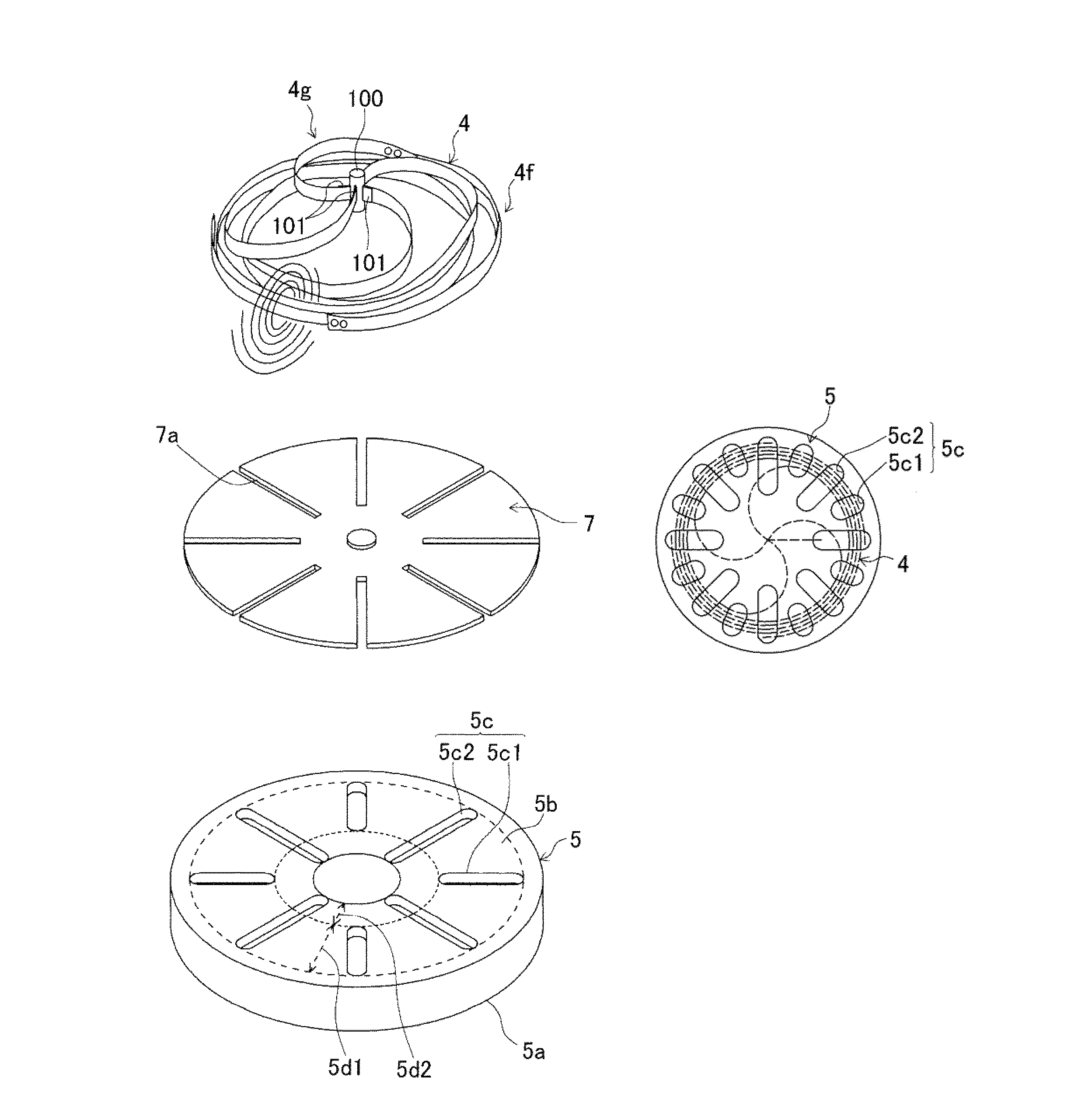
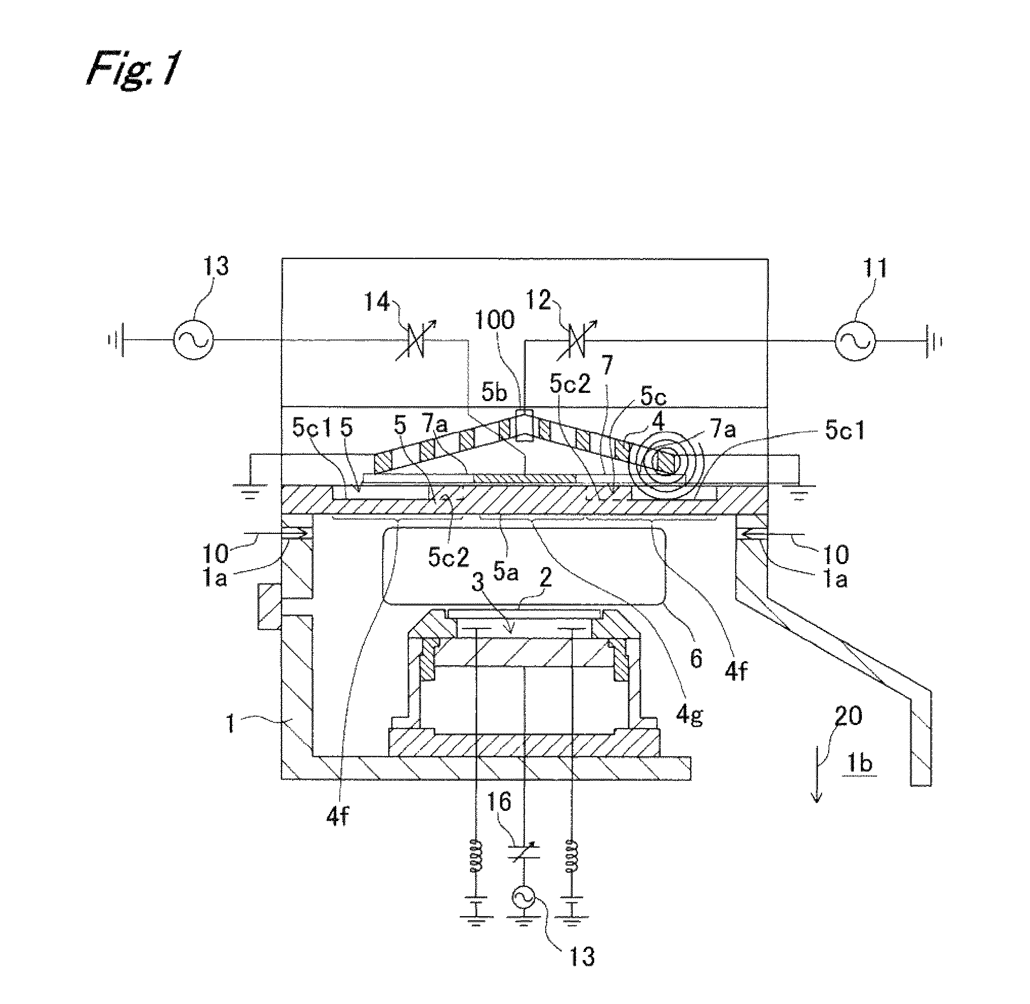
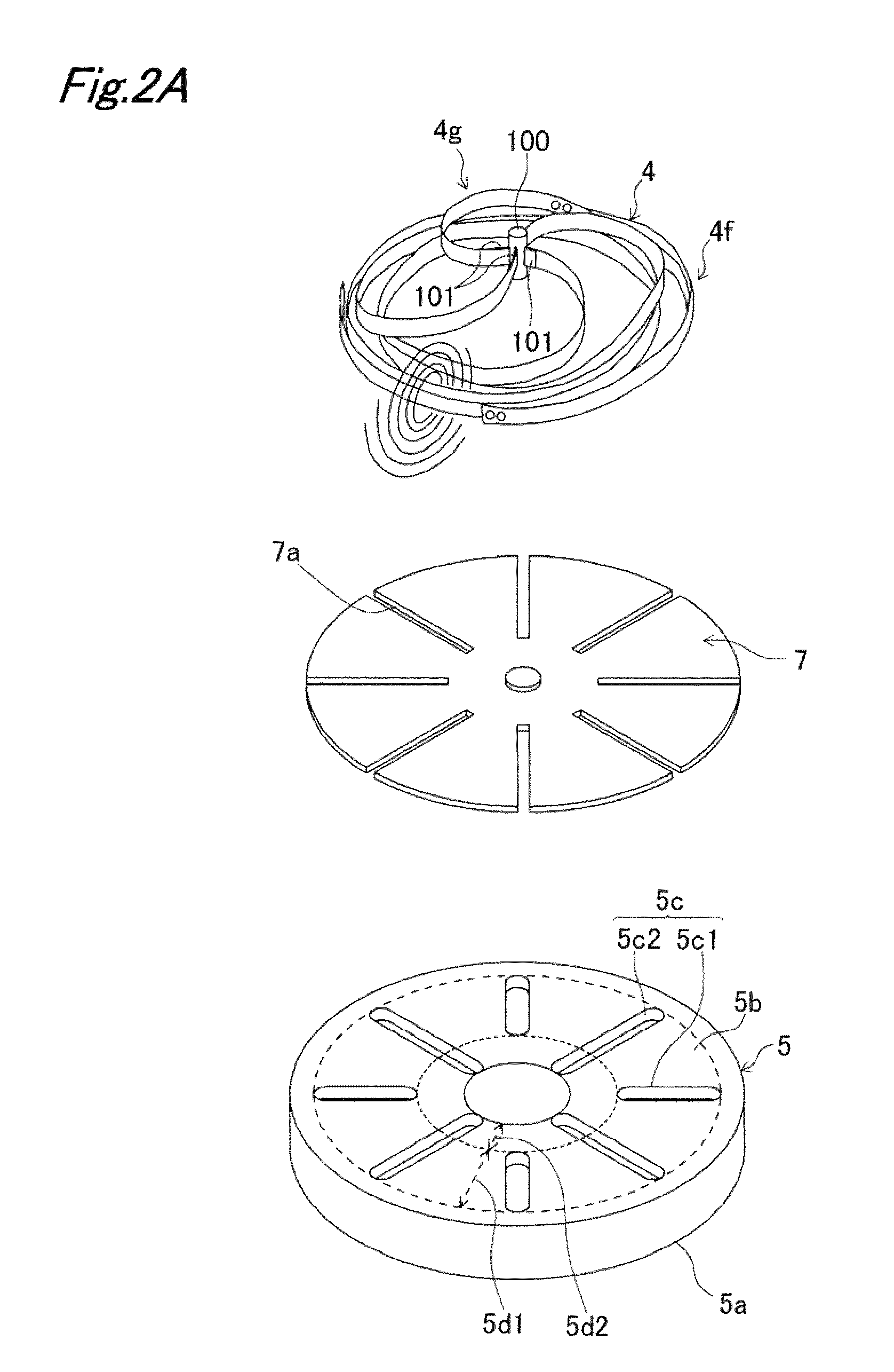
[0075]FIGS. 1 to 2B show a plasma etching apparatus according to a first embodiment of the invention. This plasma etching apparatus includes: a chamber 1 which can be depressurized and which supplies a reactant gas 10 through a supply port 1a and discharges an exhaust gas 20 through an exhaust port 1b; a placement section 3 which is provided on a lower side within the chamber 1 and which holds a placed object 2 to be treated by electrostatic attraction or clamping (not shown) or the like; and a high-withstand-pressure dielectric member 5 which forms a partition wall for sealing the upper opening of the chamber 1. The plasma etching apparatus also includes a coil 4 for inductive coupling which is provided at an upper portion of the high-withstand-pressure dielectric member 5 so as to face the placement section 3 and which transforms the reactant gas 10 within the chamber 1 into a plasma 6 by inductive coupling so that the plasma acts on the object 2 held at the placement section 3 to...

second embodiment

[0114]FIGS. 10A and 10B show a plasma etching apparatus according to a second embodiment of the invention.

[0115]Semiconductor wafers, which are objects treated by plasma processing, have been increasing in diameter more and more, as large as 200 mm to 300 mm at the present time, while the chambers for treating wafers have been further increasing in inner diameter, as large as 320 mm to 450 mm. Still more, etching has been attaining higher precision while the etching depth has also been increasing. In order to meet these requirements, there is a need for generating plasma more uniformly and more vigorously over a wide area. For this purpose, it is effective to exert a high level of radio frequency induction magnetic field or inductive coupling power from the higher-density distribution area of the coil of the peripheral-portion side annular area on the peripheral portion side of the high-withstand-pressure dielectric member in correspondence to the supply of the reactant gas into the...

third embodiment

[0126]FIG. 12 shows a plasma etching apparatus according to a third embodiment of the invention.

[0127]In this embodiment, a coil system 4a in which the number of turns is increased in the peripheral-portion side annular area, and a coil system 4b in which the number of turns is increased in the central-portion side annular area, are placed so as to be turned and expanded from different heights in upper and lower two stages, independently of each other, through a common central support shaft 100, where both coil systems 4a, 4b have their number of turns increased in one identical plane. Also, with a splitter 19 provided, radio frequency powers are supplied to the individual coil systems 4a, 4b, independently of each other, from a common power source 11. As a result of this, supply amount of the radio frequency power can be controlled for each of the coil systems 4a, 4b, i.e., for individual radial areas of the high-withstand-pressure dielectric member 5, so that plasma generated in t...


PUM

PropertyMeasurementUnit
inner diameteraaaaaaaaaa
orthogonal angleaaaaaaaaaa

Abstract

A plasma etching apparatus includes a pressure-reducible chamber 1, a placement section 3 for supporting an object to be treated within the chamber 1, a dielectric member 5 for sealing an upper opening of the chamber 1, and a coil 4 provided outside the dielectric member 5. The coil 4 generates a plasma 6 in the chamber 1 by inductive coupling so that the object 2 is subjected to etching. The dielectric member 5 has recess portions 5c discontinuous to one another. Portions of the dielectric member 5 form large-thickness portions 5b. A thickness of the dielectric member 5 in the recess portions 5c is smaller than a thickness of the large-thickness portions 5b. The recess portions 5c are placed according to distribution densities of conductors constituting the coil 4.

Description

BACKGROUND OF THE INVENTION[0001]1. Technical Field[0002]The present invention relates to plasma etching apparatuses. More specifically, the invention relates to a plasma etching apparatus including an electrode for generating plasma of a reactant gas in a chamber by inductive coupling or by inductive coupling and capacitive coupling via a high-withstand-pressure dielectric member so as to fulfill etching.[0003]2. Background Art[0004]Such plasma etching apparatuses are already known (see, e.g., Patent Literatures 1 to 3).[0005]An apparatus disclosed in Patent Literature 1 includes a metallic beam or frame body with a plurality of through windows formed therein, and a dielectric supported by the frame body to seal the chamber. Patent Literature 1 teaches as follows. With this construction, the dielectric can be reduced in thickness to thereby reduce dielectric loss, while enough pressure strength can be secured by support using a metallic beam or frame body. As a result, it becomes p...

Claims


Application Information

Patent Timeline
Patent Type & Authority Patents(United States)
IPC IPC(8): C23C16/00H01L21/306
CPCH01L21/67069H01J37/321H01L21/3065
Inventor OKITA, SHOGOWATANABE, SYOUZOUSUZUKI, HIROYUKIHOUTIN, RYUUZOU
Owner PANASONIC CORP
Why Eureka
Try Eureka