Transistor structures and methods of fabrication thereof

a transistor and structure technology, applied in the direction of transistors, thermoelectric devices, nano-informatics, etc., can solve the problems of limited charge-carrier mobility of organic materials, limited current such a transistor can provide, and less than 1 cmsup>2, and achieve the effect of reducing the operational degradation of disordered materials

Active Publication Date: 2012-11-13
TECHNION RES & DEV FOUND LTD
View PDF9 Cites 2 Cited by
  • Summary
  • Abstract
  • Description
  • Claims
  • Application Information

AI Technical Summary

Benefits of technology

[0028]The present invention, in its one aspect, solves the above problem by providing a novel electronic device (particularly a transistor structure) having a patterned electrically conductive layer, associated with either one of the active elements of the electronic device, namely source, drain or channel in case of a transistor device. The pattern is such as to form discontinuity of electrical conductivity along said layer. More specifically, the pattern (in some embodiments, nanoscale pattern) is in the form of an array (preferably two-dimensional array) of spaced-apart electrically conductive regions (e.g. islands) spaced by regions of relatively low conductivity (e.g. dielectric, or semiconducting regions). This technique provides for reducing the “effective length” of the transistor channel without any doping of the channel material.
[0053]According to yet another broad aspect of the invention, there is provided a method for use in manufacturing a vertical thin film transistor structure, the method comprising applying patterning to at least one of source and drain electrode layers to create discontinuity of electrical conductivity along said electrode, to thereby enhance the conductivity of subsequent layers in the transistor structure.
[0054]In the case of vertical TFTs, the invention provides an essentially different solution for allowing the gate voltage to affect the device current. According to the invention, a grid-like electrode (e.g. source electrode) is used, which allows the gate field flux to penetrate the source electrode layer at regions that are not covered by metal (i.e. non-conductive regions within the source electrode layer) and draw charges out of the grid to facilitate the current flow. This unique electrode structure makes the physical process driving the switch-on very different to that of [5], and facilitates a much more robust and reliable production.
[0060]The nanoscale patterns of surface energy can be used to affect the packing and film forming of semiconducting molecules such that their mobility is enhanced (better molecular packing and less uncontrolled grain boundaries).
[0061]The nanoscale patterns of surface energy can be used to create non-continuous films of solution processed semiconducting, conducting or metallic materials with a very high surface coverage (yet non-continuous to prevent electrical short). The latter can be used to effectively reduce the distance between two metallic electrodes, e.g. reduction of the effective channel length in a field-effect transistor (FET), as well as to non-uniformly dope subsequent layers. These effects can be further used to enhance the effect of non-ideal contacts to TFTs. For example, highly efficient detectors can be created by enhancing the effect of light-sensitive charge injection.

Problems solved by technology

The largest obstacle in the road to full realization of the potential is the low charge mobility restricting the flow of carriers across the channel which limits the current such a transistor can provide.
So far, the limited charge-carrier mobility of organic materials (less than 1 cm2v−1s−1) is not sufficient to provide the necessary current to the emitting diode.
The performance of organic TFTs are at best comparable to those based on amorphous silicon, and is still poor compared to inorganic crystalline material based devices.
However, is transistor design suffers from the need to produce the source electrode with a finely tuned roughness (i.e., optimization of thin versus thick properties of the film), which lowers reproducibility of these results.
Shortening the effective length that the charge needs to pass through in the semiconductor reduces the overall channel resistance and results in a higher current.
This approach is restricted by the requirement to avoid a short circuit through the conductive nanotubes, which dictates using a relatively low density of tubes.
This requirement, in turn, leads to a very limited effect.
Amorphous silicon based TFTs also typically suffer from slow switching speeds and low current handling capacity, because the electronic properties of amorphous silicon fall short of single or poly crystalline silicon.
All these solutions require significant research and changes to existing production lines.

Method used


Image

  • Transistor structures and methods of fabrication thereof
  • Transistor structures and methods of fabrication thereof
  • Transistor structures and methods of fabrication thereof

Examples


Embodiment Construction

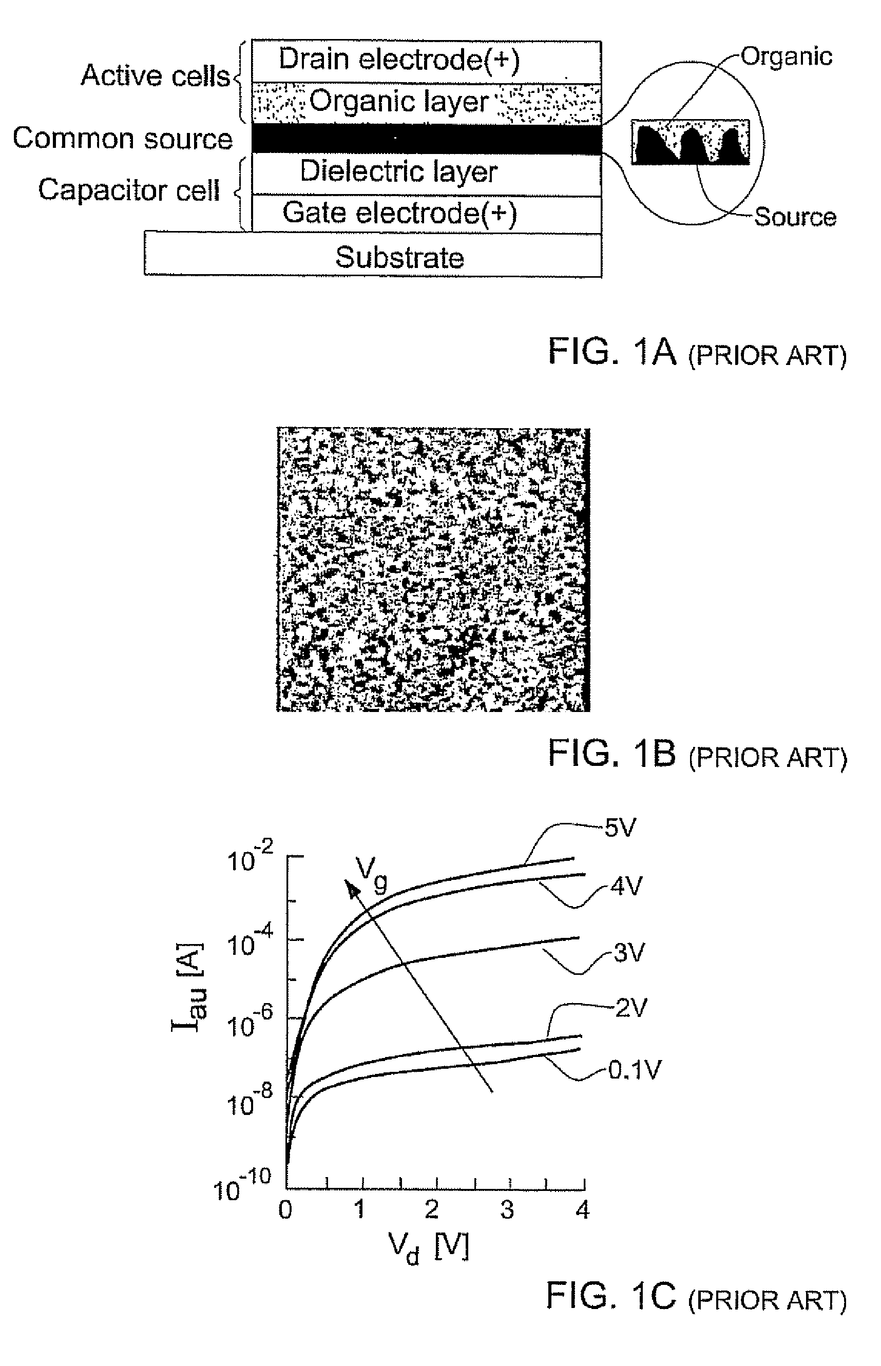
[0089]FIGS. 1a-b show the known gate-source-drain vertical organic field effect transistor (VOFET) structure described in the above-indicated article of L. Ma and Y. Yang, “Unique architecture and concept for high-performance organic transistors”, Applied Physics Letters 85, 5084-5086 (2004)]. FIG. 1c shows the VOFET conductance characteristics for different gate-source voltage.

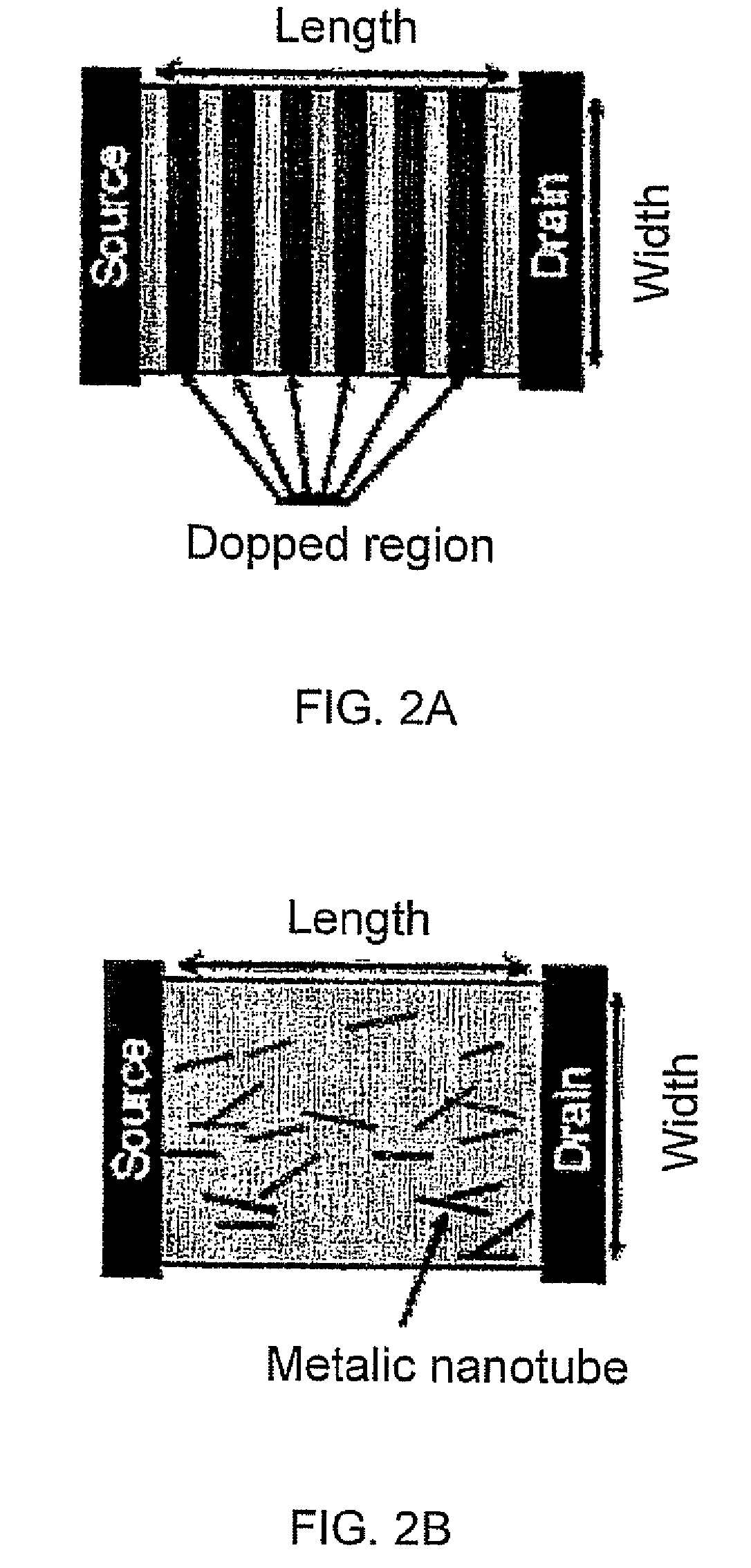
[0090]FIGS. 2a and 2b illustrate the known planar transistors described in [6, 7].

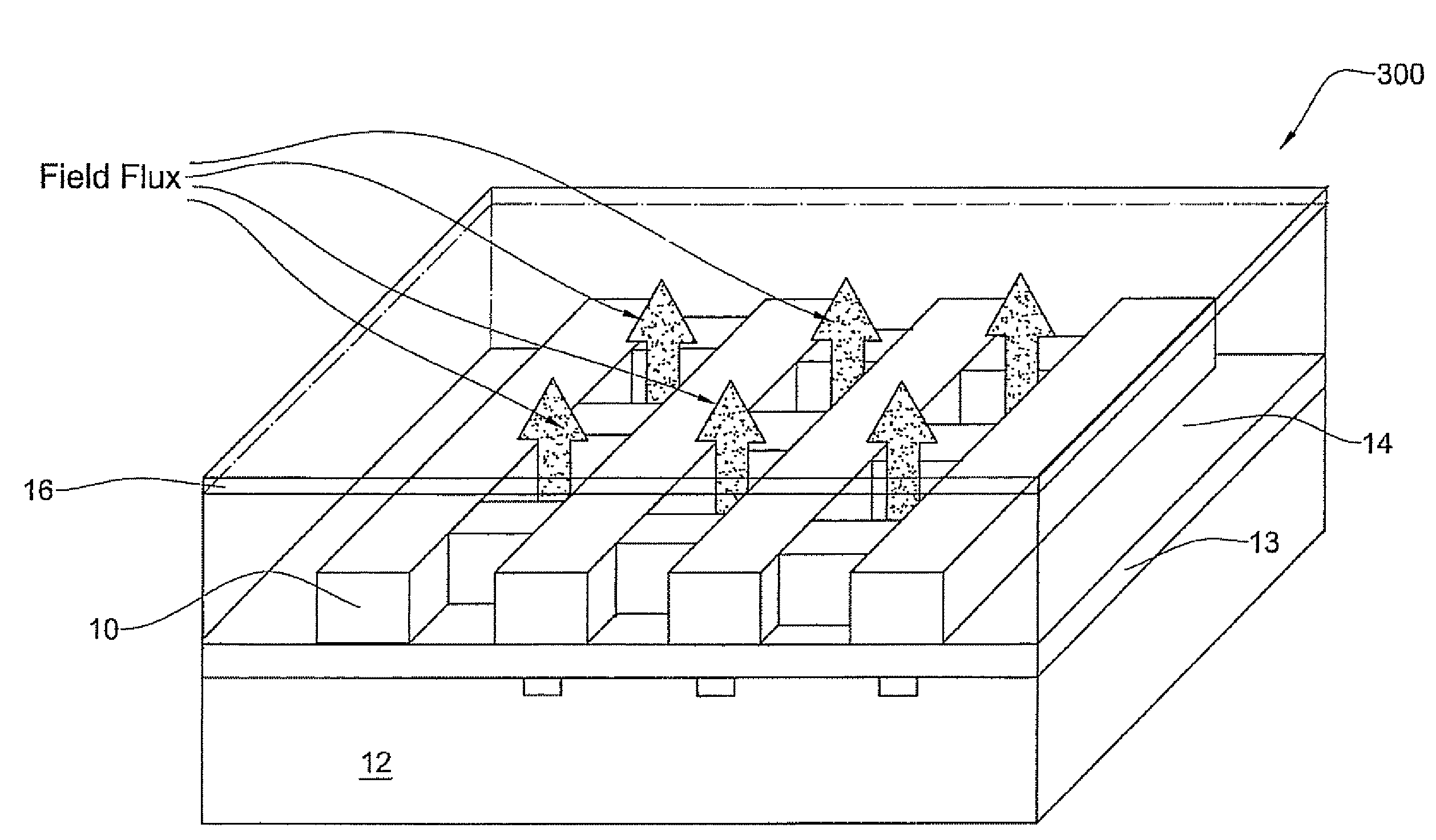
[0091]The present invention, according to its one aspect, provides a novel transistor structure having a patterned electrically-conductive layer associated with an active element of the transistor. This electrically-conductive layer has a two-dimensional pattern defining spaced-apart electrically conductive regions. This allows for increasing an electric current through the transistor, as well as a switching speed thereof.

[0092]The invention can be used in vertical configuration transistors and in lateral configuration transisto...


PUM

PropertyMeasurementUnit
thicknessaaaaaaaaaa
channel currentaaaaaaaaaa
heightaaaaaaaaaa

Abstract

An electronic device is presented, such as a thin film transistor. The device comprises a patterned electrically-conductive layer associated with an active element of the electronic device. The electrically-conductive layer has a pattern defining an array of spaced-apart electrically conductive regions. This technique allows for increasing an electric current through the device.

Description

FIELD OF THE INVENTION[0001]The present invention is generally in the field of designing electronic device architectures. More specifically the invention relates to thin film transistors for use, for example, in organic electronics, display devices and detectors.REFERENCES[0002]The following references are considered to be pertinent for the purpose of understanding the background of the present invention:[0003]1. H. Siringhaus, N. Tessler, and R. H. Friend, Science 280, 1741-1743 (1998);[0004]2. N. Stutzmann et al., “Self-aligned, vertical-channel, polymer field-effect transistors” Science 299, 1881-1884 (2003);[0005]3. S. Tanaka et al “Vertical- and lateral-type organic FET using pentacene evaporated films,”Electrical Engineering in Japan, vol. 149, pp. 43-48, 2004;[0006]4. J. I. Nishizawa, T. Terasaki, and J. Shibata, “Field-Effect Transistor Versus Analog Transistor (Static Induction Transistor),”Ieee Transactions on Electron Devices, vol. ED22, pp. 185-197, 1975;[0007]5. L. Ma a...

Claims


Application Information

Patent Timeline
Patent Type & Authority Patents(United States)
IPC IPC(8): H01L35/24
CPCB82Y10/00H01L51/0021H01L51/004H01L51/0043H01L29/786H01L51/0516H01L51/0558H01L51/057H01L51/102H01L51/0046H10K71/60H10K85/141H10K85/151H10K85/211H10K10/468H10K10/491H10K10/484H10K10/82H10K10/46H10K10/40H10K10/466H10K10/464H10K50/11H10K85/113
Inventor TESSLER, NIRMARGALIT, MOTIGLOBERMAN, ODEDSHEHHAR, ROY
Owner TECHNION RES & DEV FOUND LTD
Why Eureka
Try Eureka