Charged particle apparatus

a particle apparatus and charge technology, applied in the field of charge particle apparatus, can solve the problems of increasing the complexity and instability of the system, reducing the yield to a great degree, and increasing the chromatic aberration disc and spherical aberration disc, so as to achieve low aberration, improve the spatial resolution, and reduce the effect of aberration

Active Publication Date: 2012-11-27
ASML NETHERLANDS BV
View PDF15 Cites 5 Cited by
  • Summary
  • Abstract
  • Description
  • Claims
  • Application Information

AI Technical Summary

Benefits of technology

[0014]The object of this invention is to provide an electron beam apparatus employing LVSEM technology. In this apparatus, by specifically arranging the electron deceleration and the overlap of the retarding field and the magnetic objective field, the electromagnetic compound objective lens is designed to have lower aberrations and low coil excitation. So, this invention can provide a higher spatial resolution with a probe current larger than before, which can especially benefit the defect inspection and review in semiconductor yield management.

Problems solved by technology

In semiconductor manufacture, pattern defects occur on the mask or wafer during the fabrication process, which reduce the yield to a great degree.
Obviously, the chromatic aberration disc, diffraction disc and Coulomb effect become larger at low energy V. The only way to reduce the diffraction disc is using a bigger half angle, but unfortunately this will increase chromatic aberration disc and spherical aberration disc at the same time.
However, such a design will require a larger coil excitation (product of coil turns and coil current), because only a part of the magnetic field located in front of the specimen surface takes part the particle beam focusing.
A larger coil excitation incurs heat conduction and cooling issue, and solving this issue increases complexity and instability of the system.

Method used


Image

  • Charged particle apparatus
  • Charged particle apparatus
  • Charged particle apparatus

Examples


Embodiment Construction

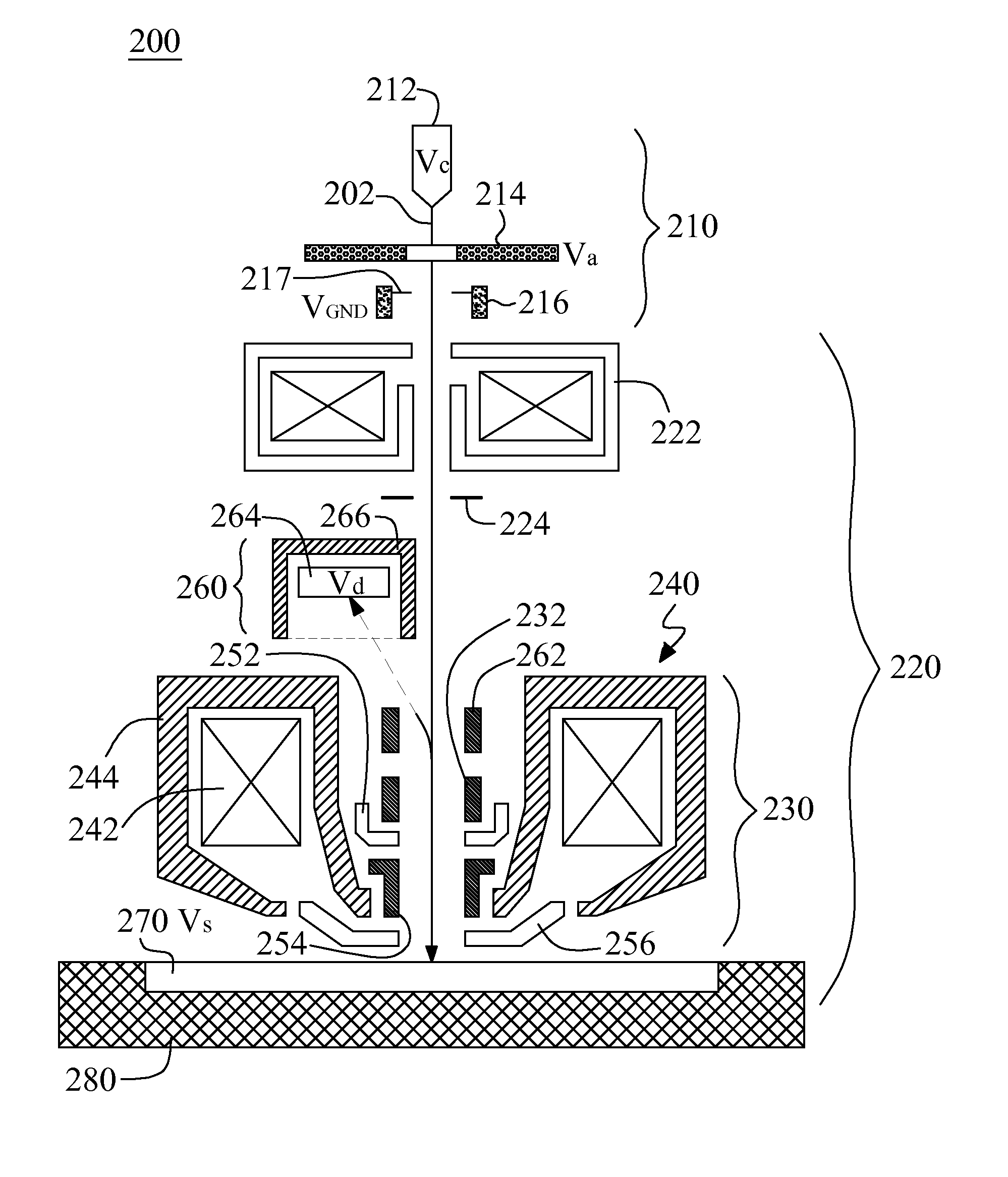
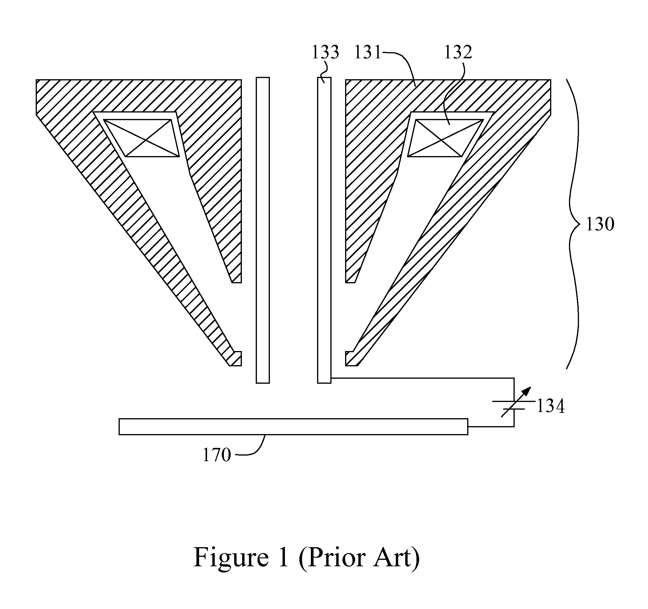
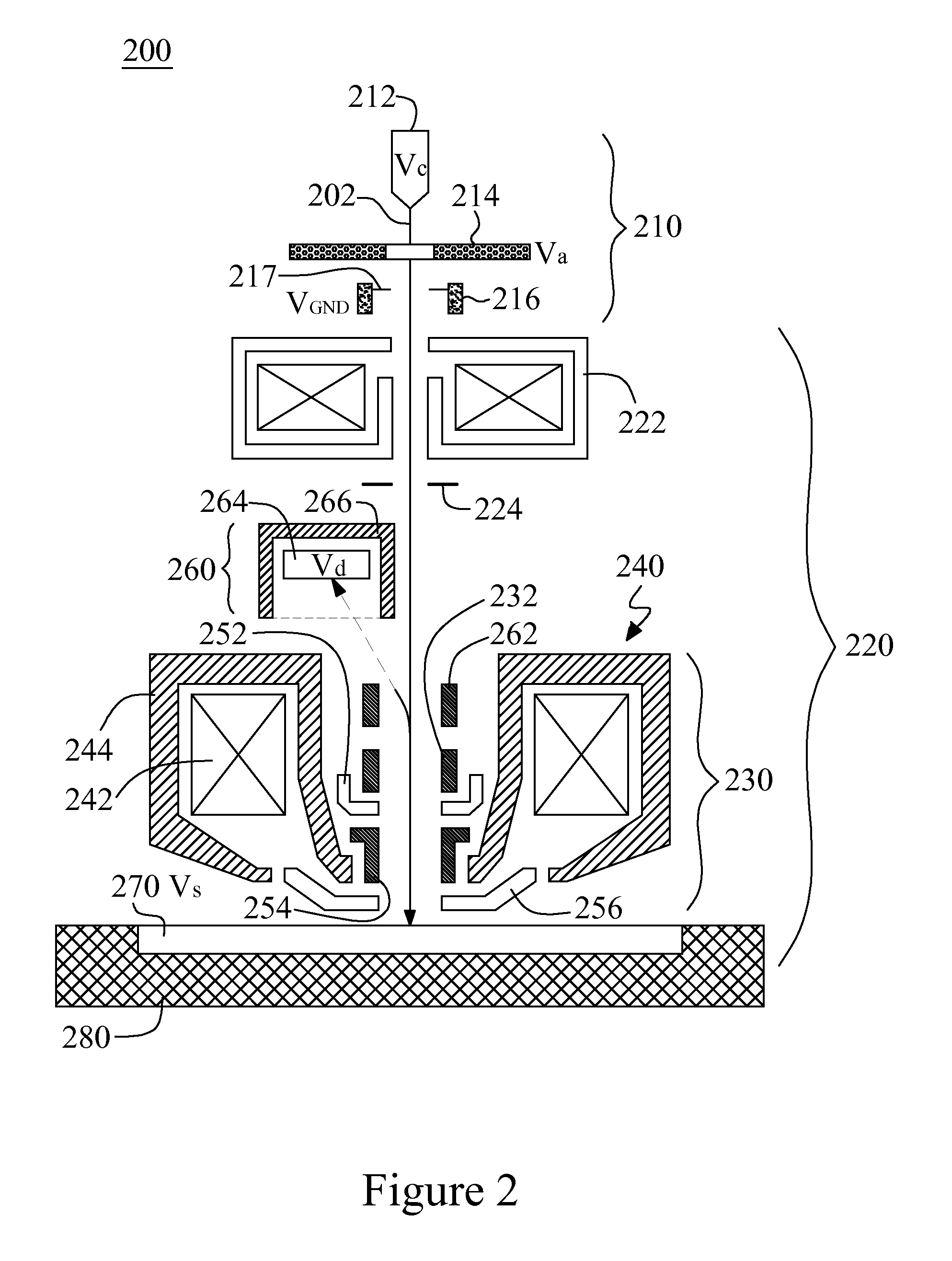
[0031]Various example embodiments of the present invention will now be described more fully with reference to the accompanying drawings in which some example embodiments of the invention are shown. In the drawings, relative dimensions of each component and among every component may be exaggerated for clarity.

[0032]Detailed illustrative embodiments of the present invention are disclosed herein. However, specific structural and functional details disclosed herein are merely representative for purposes of describing example embodiments of the present invention. This invention, however, may be embodied in many alternate forms and should not be construed as limited to only the embodiments set forth herein.

[0033]Accordingly, while example embodiments of the invention are capable of various modifications and alternative forms, embodiments thereof are shown by way of example in the drawings and will herein be described in detail. It should be understood, however, that there is no intent to ...


PUM


Abstract

An electromagnetic compound objective lens is provided for charged particle device, especially as an objective lens of low-voltage scanning electron microscope (LVSEM), which comprises a magnetic immersion lens and an electrostatic immersion lens. The magnetic immersion lens orients its gap between an inner pole piece and an outer pole piece to specimen's surface, and uses a magnetic specimen stage. The electrostatic immersion lens comprises three or four electrodes which apply suitable retarding field to a primary beam of the charged particle device for reducing its landing energy on specimen surface and further eliminating imaging aberrations.

Description

BACKGROUND OF THE INVENTION[0001]1. Field of the Invention[0002]The present invention relates to a charged particle apparatus, and more particularly to an immersion electromagnetic compound objective lens for a charged particle apparatus.[0003]2. Description of Related Art[0004]In semiconductor manufacture, pattern defects occur on the mask or wafer during the fabrication process, which reduce the yield to a great degree. Defect inspection, and defect review are widely used for yield management. High spatial resolution, high throughput and low radiation damage on specimen are the major determinants when judging their performance. For the defect inspection and review systems with high spatial resolution, Low-voltage Scanning Electron Microscopy (LVSEM) with Field Emission Source (FES) has been the core technology because of its high spatial resolution and low radiation damage on specimen.[0005]Different from a conventional Scanning Electron Microscope (SEM), in a LVSEM, the examined ...

Claims


Application Information

Patent Timeline
Patent Type & Authority Patents(United States)
IPC IPC(8): H01J37/145
CPCH01J37/141H01J37/28H01J37/145
Inventor REN, WEIMING
Owner ASML NETHERLANDS BV
Why Eureka
Try Eureka