

Phase-locked loop circuit and communication apparatus
a phase-locked loop and communication device technology, applied in the direction of electrical devices, pulse automatic control, angle demodulation by phase difference detection, etc., can solve the problem of large circuit area, and achieve the effect of low power consumption and miniaturization
- Summary
- Abstract
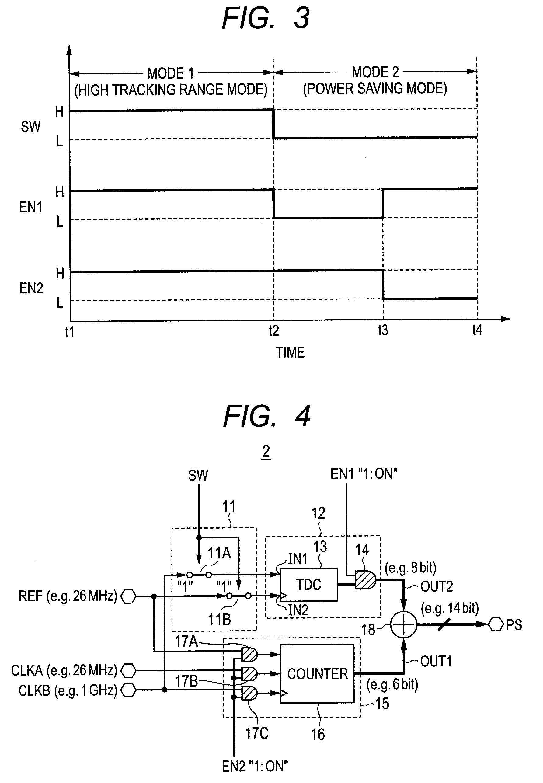
- Description
- Claims
- Application Information
AI Technical Summary
Benefits of technology
Problems solved by technology
Method used
Image

Examples
embodiment 1
[0047](Embodiment 1)
[0048](Configuration of ADPLL Circuit 1)
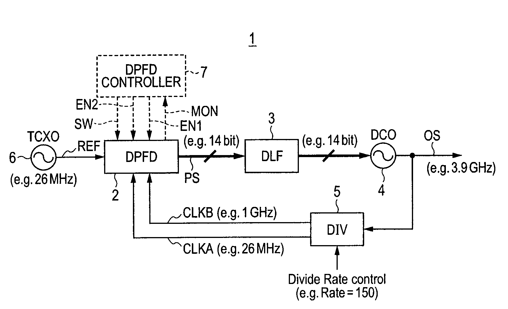
[0049]FIG. 1 is a block diagram illustrating configuration of an ADPLL circuit 1 according to Embodiment 1 of the present invention. In FIG. 1, an ADPLL circuit 1 corresponds to a circuit which generates a highly-accurate high frequency clock in an RF-IC chip, for example. The ADPLL circuit 1 includes a digital controlled oscillator (DC0) 4, a divider (DIV) 5, a digital phase-frequency detector (DPFD) 2, and a digital loop filter (DLF) 3.
[0050]The digital controlled oscillator 4 oscillates at a frequency corresponding to a digital output of the digital loop filter 3. Publicly known configuration can be employed for the digital controlled oscillator 4. For example, a ring oscillator composed of plural inverters is known as a digital controlled oscillator. In this case, corresponding to the multi-bit digital output of the digital loop filter 3, the inverters are individually controlled to turn into an active state or a non-ac...
embodiment 2
[0191](Embodiment 2)
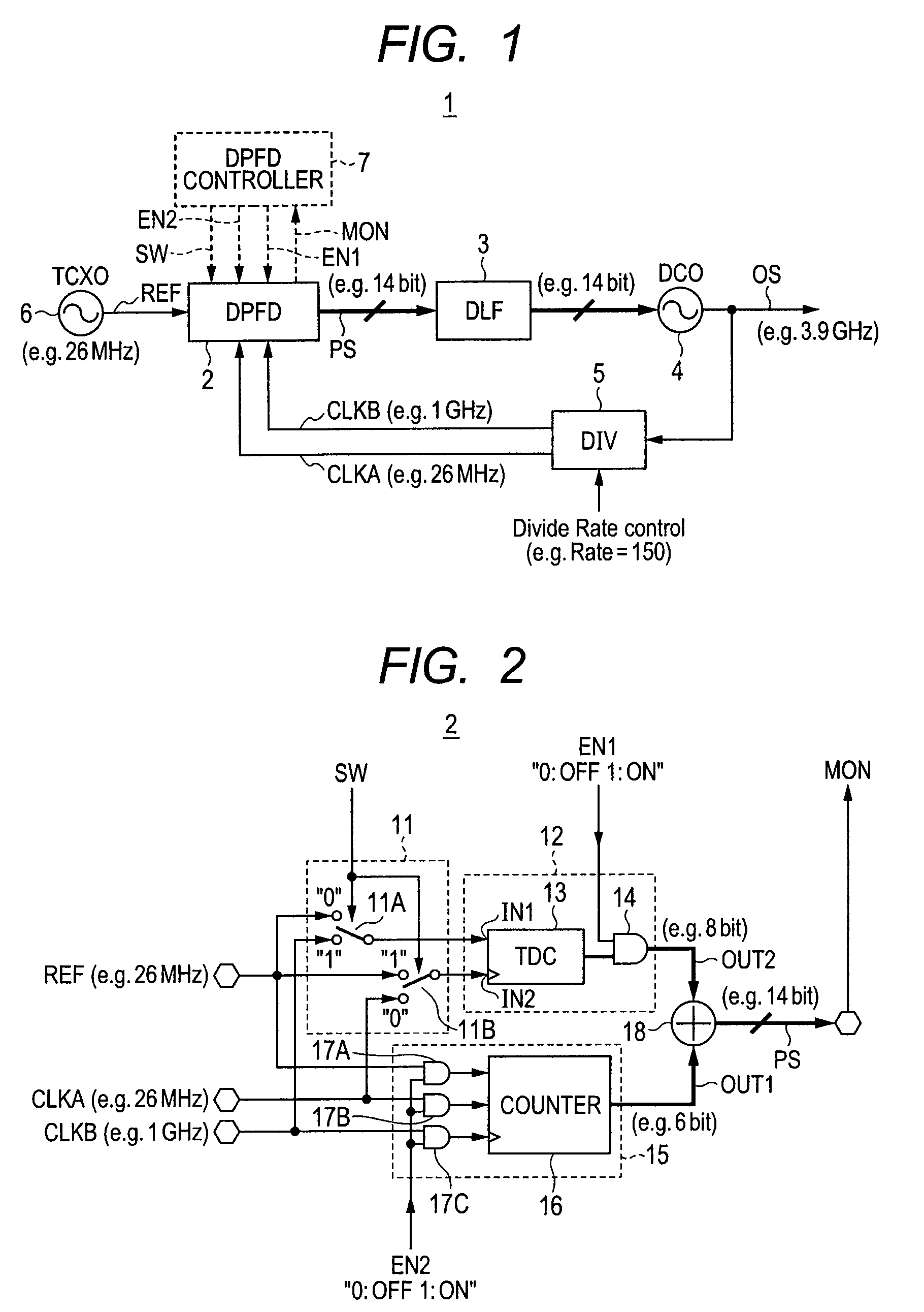
[0192]FIG. 22 is a block diagram illustrating configuration of a digital phase-frequency detector 2A according to Embodiment 2 of the present invention.
[0193]The digital phase-frequency detector 2A illustrated in FIG. 22 differs from the digital phase-frequency detector 2 illustrated in FIG. 2 in that a phase determination unit 41 (PFD) is further included in the input side of a switch 11A. The phase determination unit 41 receives the reference clock signal REF and the low frequency clock signal CLKA. When the control signal SW is “0” (Mode 2), an output of the phase determination unit 41 is inputted into an input node IN1 of a time-to-digital converter 13 via the switch 11A. When the control signal SW is “1” (Mode 1), the high frequency clock signal CLKB is inputted into the input node IN1 of the time-to-digital converter 13 via the switch 11A, same as in the case of FIG. 2. As for the other portions, the digital phase-frequency detector 2A illustrated in FIG. 2...
embodiment 3
[0201](Embodiment 3)
[0202]It is assumed that locking of the PLL frequency synthesizer has established at a time when the phase difference (time difference) between the reference clock signal REF and the low frequency clock signal CLKA is approximately zero. In this case, when the phase difference shifts to the minus side due to disturbance, such as a temperature change, the value of the output of the digital phase-frequency detector 2 will change rapidly, as the graph of the input-output characteristics of FIG. 14 indicates. As a result, the locking of the PLL frequency synthesizer may be freed, causing a problem. In Embodiment 3, offsets are added to the outputs of the counter 16 and the time-to-digital converter 13, so that the outputs of the counter 16 and the time-to-digital converter 13 may lock at the center of the respective linear output range.
[0203]FIG. 25 is a block diagram illustrating configuration of a digital phase-frequency detector 2B according to Embodiment 3 of the...
PUM
 Abstract
Description
Claims
Application Information