Systems, methods, and apparatuses for complementary metal oxide semiconductor (CMOS) driver circuits using shared-charge recycling charge pump structures

a technology of complementary metal oxide semiconductors and charge pump structures, which is applied in logic circuits, pulse techniques, reliability increasing modifications, etc., can solve the problems of power consumption, ever shrinking feature size of a cmos technology, and reducing the power supply voltage, so as to reduce the power consumption of the charge pump, reduce the power consumption, and sacrifice the output voltage level

Active Publication Date: 2012-12-18
SAMSUNG ELECTRO MECHANICS CO LTD
View PDF2 Cites 8 Cited by
  • Summary
  • Abstract
  • Description
  • Claims
  • Application Information

AI Technical Summary

Benefits of technology

[0007]In an example embodiment of the invention, an example shared-charge recycling process may be utilized with an antenna-switch driver circuit. More specifically, an example shared-charge recycling process may be applied to a clock buffer and charge transfer cells of the charge pump in the antenna-switch driver circuit. An example recycling process may include recycling of shared charges between the capacitors in the charge transfer cells. In contrast to prior art charge pump circuits with the CMOS-inverter clock buffers where the charges stored in the capacitors of the charge transfer cells are discharged directly to ground and wasted, an example recycling process may use the charges in on

Problems solved by technology

Due to the increased demand for mobile devices, power consumption has been a major concern in designing integrated circuits, especially for driver circuits to drive antenna switches, liquid crystal displays (LCDs), and memories because these components are integrated in one mobile device to satisfy the customers' demand on functionalities.
The integration of these various functional blocks, typically d

Method used


Image

  • Systems, methods, and apparatuses for complementary metal oxide semiconductor (CMOS) driver circuits using shared-charge recycling charge pump structures
  • Systems, methods, and apparatuses for complementary metal oxide semiconductor (CMOS) driver circuits using shared-charge recycling charge pump structures
  • Systems, methods, and apparatuses for complementary metal oxide semiconductor (CMOS) driver circuits using shared-charge recycling charge pump structures

Examples


example measurement

[0045 Results

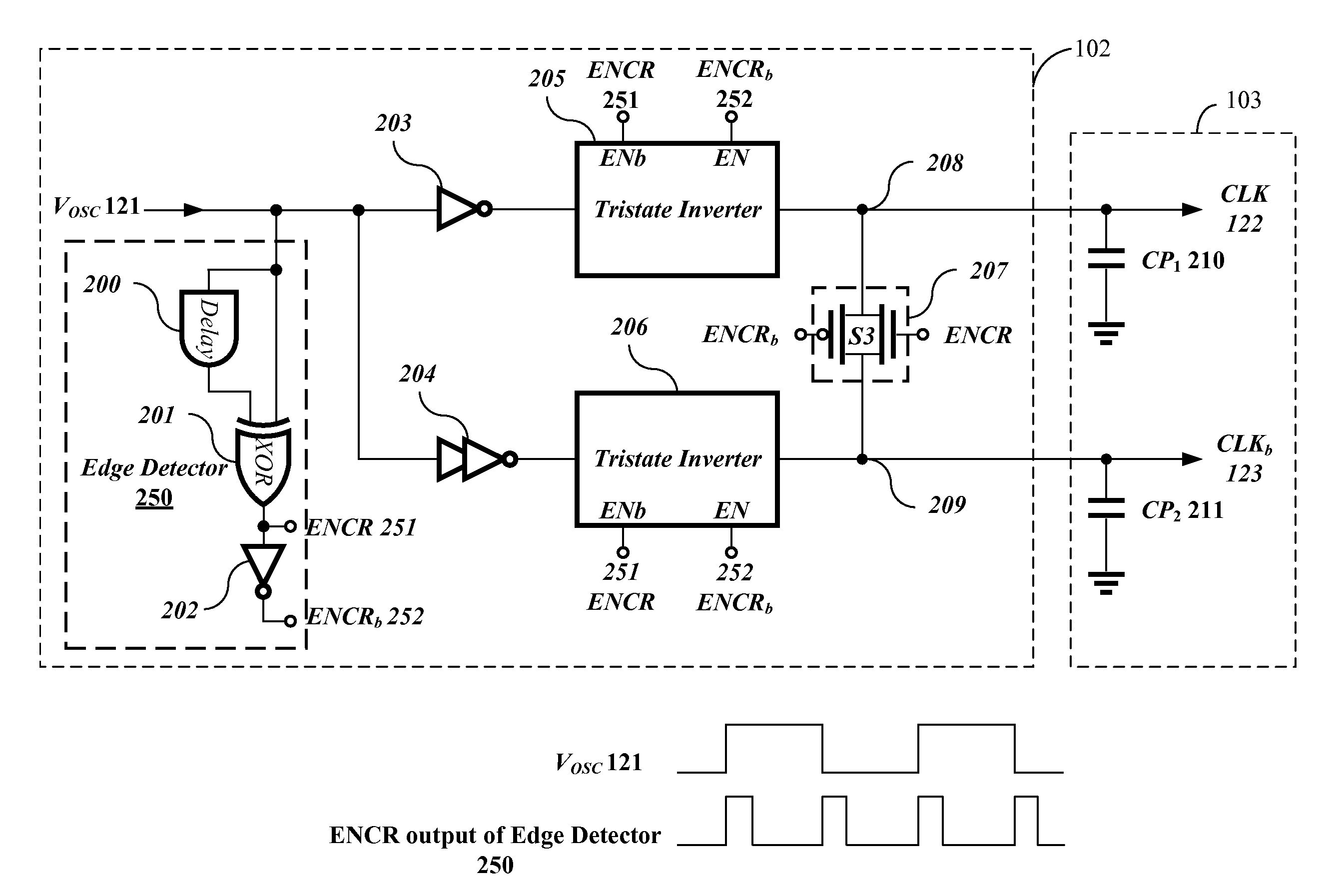
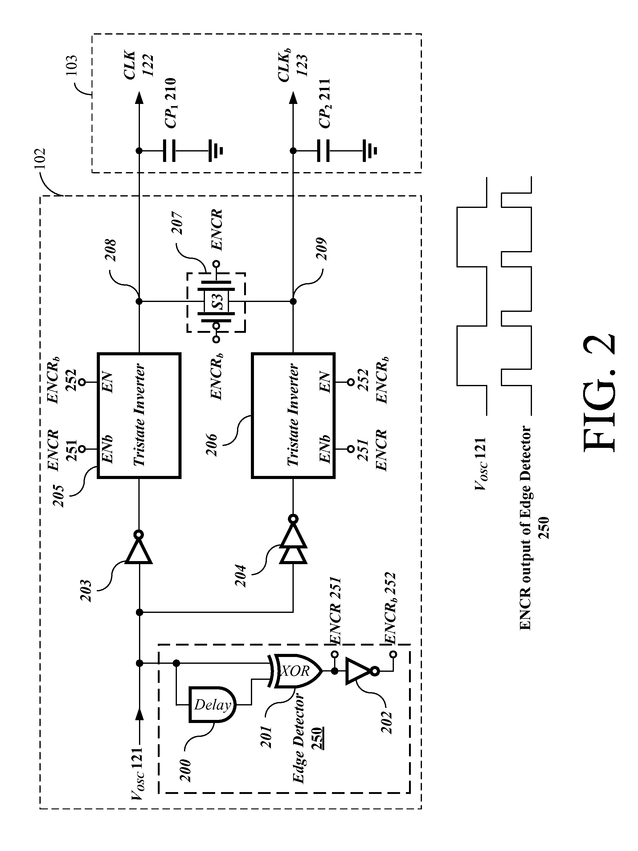
[0046]FIG. 7 illustrates example measurement results for the operation of an example shared-charge recycling process in accordance with an embodiment of the invention. These measurement results illustrate the current reduction obtained by using the shared-charge recycling technique. FIG. 7 illustrates the current consumption 701 of the antenna-switch driver with an example shared-charge recycling process and the current consumption 700 without the shared-charge recycling process 700. As shown by FIG. 7, the current consumption 701 utilizing the shared-charge recycling process may be reduced compared to the current consumption 700. FIG. 8 illustrates the percentage of the amount of reduced current that is realized based upon an example shared-charge recycling process, according to an example embodiment of the invention.


PUM


Abstract

Example driver circuits can utilize shared-charge recycling charge pump structures. In particular, an example shared-charge recycling process may be applied to a clock buffer and charge transfer cells of the charge pump in a driver circuit. An example recycling process may include recycling of shared charges between the capacitors/capacitances in the charge transfer cells. An example recycling process may use the charges in one or more capacitors to charge one or more other capacitors before the charges are wasted or otherwise discharged to ground. Such recycling may significantly reduce the power consumption of the charge pump while still providing a high output voltage level, according to an example embodiment of the invention.

Description

FIELD OF THE INVENTION[0001]Aspects of the invention relate generally to driver circuits, and more particularly, to complementary metal-oxide-semiconductor (CMOS) driver circuits using shared-charge recycling pump structures.BACKGROUND OF THE INVENTION[0002]Due to the increased demand for mobile devices, power consumption has been a major concern in designing integrated circuits, especially for driver circuits to drive antenna switches, liquid crystal displays (LCDs), and memories because these components are integrated in one mobile device to satisfy the customers' demand on functionalities. The integration of these various functional blocks, typically digital blocks, led to the ever-shrinking feature size of a CMOS technology, and the scaling-down resulted in a lower power-supply voltage. However, many driver circuits still need a higher voltage than a given power-supply voltage. In addition, a negative voltage is necessary for many applications, which include memories and antenna...

Claims


Application Information

Patent Timeline
IPC IPC(8): H03K19/00H03K19/02
CPCH03K19/0019
Inventor CHA, JEONGWONSONG, TAEJOONGCHO, CHANGHYUKAHN, MINSIKLEE, CHANG-HOWOO, WANGMYONGCHANG, JAE JOON
Owner SAMSUNG ELECTRO MECHANICS CO LTD
Why Eureka
Try Eureka