
Semiconductor device with reduced junction leakage and an associated method of forming such a semiconductor device

a semiconductor device and junction leakage technology, applied in the field of semiconductor devices, can solve the problems of non-functional devices, complex devices, and design of p-n junctions in such devices, and achieve the effects of reducing leakage, reducing leakage, and increasing the schottky barrier heigh

Inactive Publication Date: 2013-01-08
GLOBALFOUNDRIES U S INC +1
View PDF6 Cites 7 Cited by
  • Summary
  • Abstract
  • Description
  • Claims
  • Application Information

AI Technical Summary

Benefits of technology

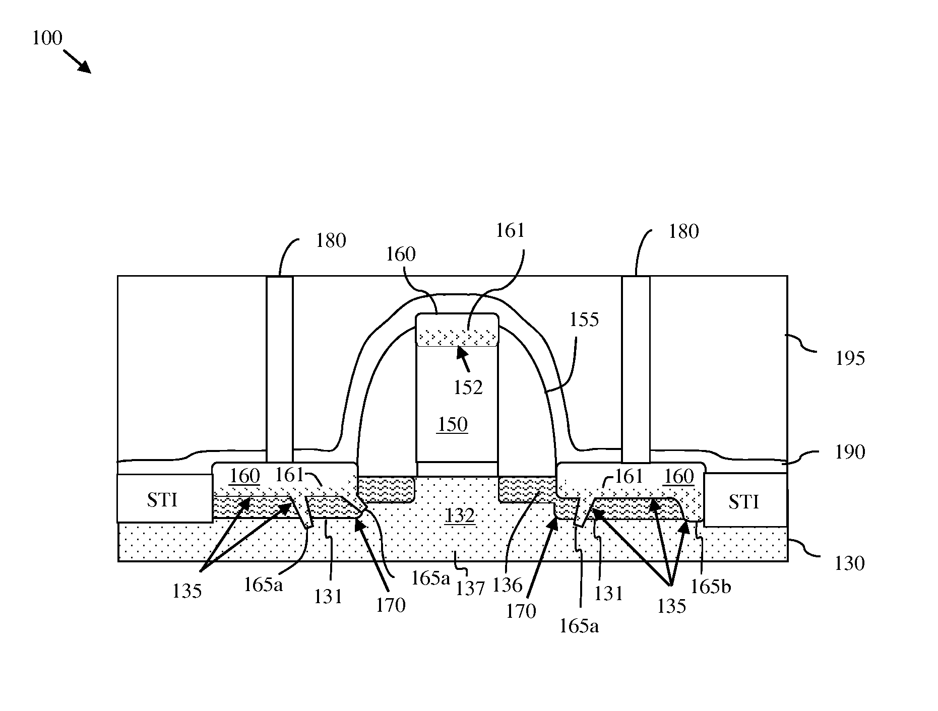
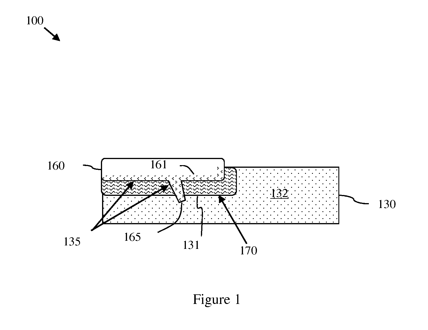
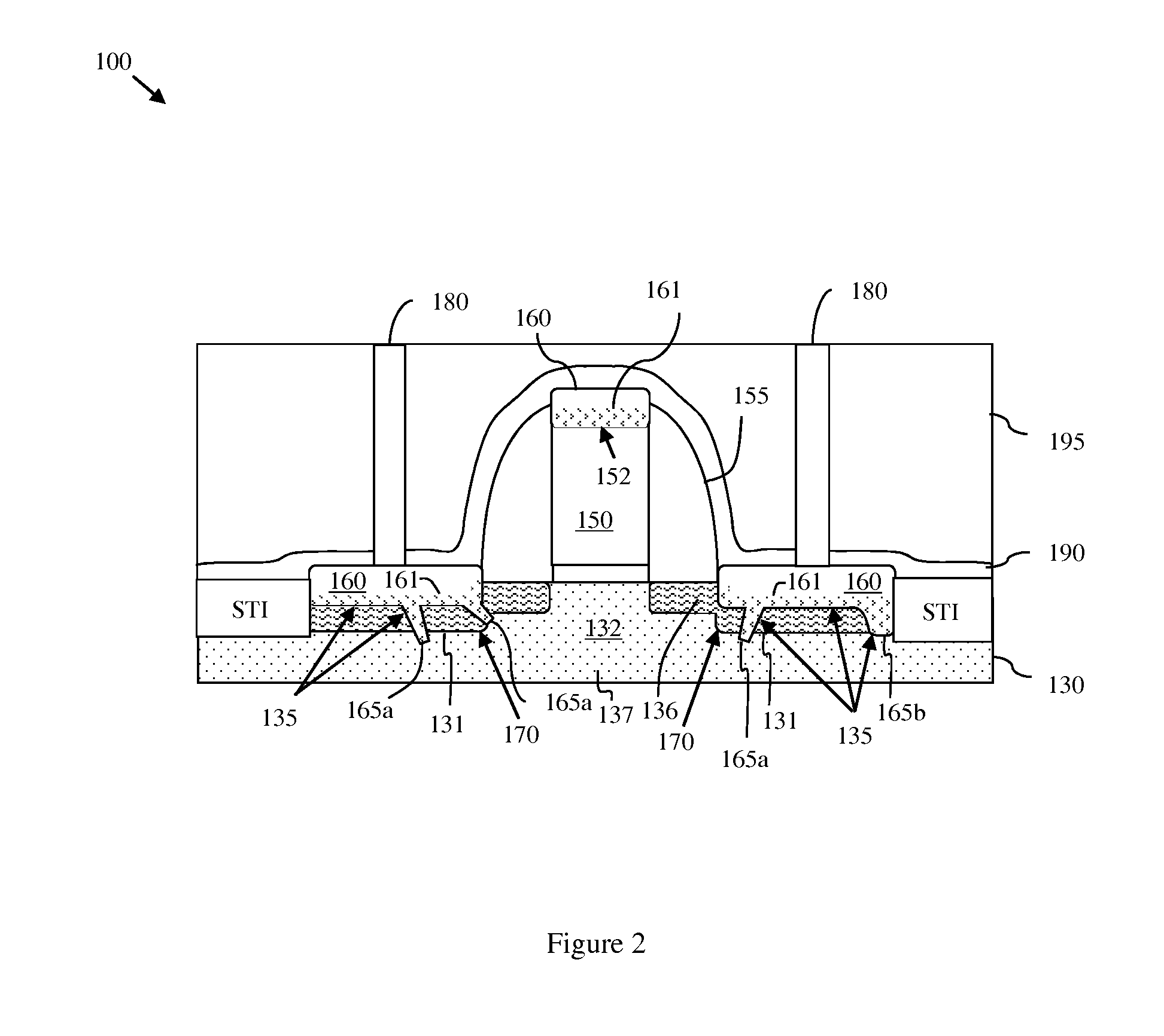
[0006]Specifically, the embodiments of the semiconductor device can comprise a semiconductor layer. The semiconductor layer can comprise a p-n junction. That is, the semiconductor layer can comprise a first semiconductor region and a second semiconductor region adjacent to the first semiconductor region. The first semiconductor region can be doped with a first dopant having a first conductivity type and the second semiconductor region can be doped with a second dopant having a second conductivity type that is different from the first conductivity type. Additionally, the semiconductor device can comprise a metal silicide layer on a surface of the first semiconductor region. This metal silicide layer comprise at least one metal silicide defect extending through the first semiconductor region to the second semiconductor region (i.e., contacting or traversing the p-n junction). The metal silicide layer can be doped with a third dopant. The concentration profile of the third dopant within the metal silicide layer can be such that the peak concentration of the third dopant is located within the portion of the metal silicide layer that borders the interface between the metal silicide layer and the semiconductor layer and, thus, encompasses the metal silicide defect(s). The third dopant can be preselected to have either the same conductivity type as the first dopant or to have neither the first conductivity type, nor the second conductivity type, such that a relatively high concentration of this third dopant within the metal silicide defect(s) effectively blocks any junction leakage which would otherwise occur when the junction is in reverse polarity (i.e., in a reverse biased situation). More specifically, the third dopant can be preselected such that, due to the peak concentration of the third dopant being within the metal silicide defect(s), the silicide to silicon contact is effectively engineered to increase the Schottky barrier height at the defect, which in turn drastically reduces any leakage that would otherwise occur, when the p-n junction is in reverse polarity. In one exemplary embodiment, the above-described semiconductor device can comprise a field effect transistor with a source / drain to channel p-n junction having reduced leakage even in the presence of metal silicide defect(s) that reach the junction.
[0007]Embodiments of a method of forming a semiconductor device, as described above, having a p-n junction with reduced junction leakage even in the presence of metal silicide defect(s) that reach the junction can comprise forming a semiconductor layer with a p-n junction. That is, the method embodiments can comprise forming a semiconductor layer comprising a first semiconductor region and a second semiconductor region adjacent to the first semiconductor region, where the first semiconductor region has a first conductivity type and the second semiconductor region has a second conductivity type different from the first conductivity type. Next, a metal silicide layer can be formed on a surface of the first semiconductor region and a dopant can be implanted into the metal silicide layer. This dopant can be preselected to have the same conductivity type as the first semiconductor region (i.e., the first conductivity type) or to have neither the first conductivity type, nor the second conductivity type. Then, an anneal process can be performed so as to cause the dopant within the metal silicide layer to migrate toward the interface between the metal silicide layer and the semiconductor layer, preferably, without crossing over the interface. This anneal process is specifically performed to adjust the concentration profile of the dopant within the metal silicide layer so as to ensure that the peak concentration of the dopant is within the portion of the metal silicide layer bordering the interface. It should be noted that this portion of the metal silicide layer with the peak concentration of the dopant will necessarily encompass any metal silicide defect created during the metal silicide formation process and extending through the first semiconductor region to the second semiconductor region (i.e., contacting or traversing the p-n junction). Thus, if any metal silicide defects are created during the metal silicide formation process, the relatively high concentration of dopant forced into those defects will effectively block any junction leakage that would otherwise occur when the junction is in reverse polarity (i.e., in a reverse biased situation). More specifically, due to the peak concentration of the dopant being within the metal silicide defect(s) that extend to the p-n junction, the silicide to silicon contact is effectively engineered to increase the Schottky barrier height at the defect, which in turn drastically reduces any leakage that would otherwise occur, when the p-n junction is in reverse polarity.
[0008]In one exemplary method embodiment, the semiconductor device that is formed can comprise a field effect transistor with a source / drain to channel p-n junction having reduced leakage even in the presence of metal silicide defects that extend to (i.e., contact or traverse) the junction. Specifically, in this exemplary method embodiment, a semiconductor layer with a source / drain to channel p-n junction can be formed. That is, a semiconductor layer can be formed such that it comprises a source / drain region and a channel region adjacent to the source / drain region, where the source / drain region is doped with a first dopant, having a first conductivity type, and the channel region is doped with a second dopant, having a second conductivity type. A dopant activation anneal process (e.g., a thermal anneal process) can be performed so as to activate the first dopant in the source / drain region and the second dopant in the channel region. After the dopant activation anneal process is performed, a metal silicide layer can be formed on a surface of the source / drain region. Then, a third dopant can be implanted into the metal silicide layer. This third dopant can be preselected either to have the same conductivity type as the first dopant (i.e., the first conductivity type) or to have neither the first conductivity type, nor the second conductivity type. Then, an additional anneal process (e.g., an additional thermal anneal process, a laser anneal process, a flash anneal process, etc.) can be performed so as to cause the third dopant within the metal silicide layer to migrate toward the interface between the metal silicide layer and the semiconductor layer, preferably, without crossing over the interface. This additional anneal process can specifically be performed to adjust the concentration profile of the third dopant in the metal silicide layer so as to ensure that the peak concentration of the third dopant is within the portion of the metal silicide layer bordering the interface. It should be noted that this portion of the metal silicide layer having the peak concentration of the third dopant will necessarily encompass any metal silicide defect created during metal silicide formation and extending through the source / drain region to the channel region (i.e., contacting or traversing the source / drain to channel p-n junction). Thus, if any metal silicide defects are created during metal silicide formation, the relatively high concentration of the third dopant forced into those defects will effectively block any junction leakage that would otherwise occur when the junction is in reverse polarity (i.e., in a reverse biased situation). More specifically, due to the peak concentration of the third dopant being within the metal silicide defect(s) that extend to the source / drain to channel p-n junction, the silicide to silicon contact is effectively engineered to increase the Schottky barrier height at the defect, which in turn drastically reduces any leakage that would otherwise occur, when the p-n junction is in reverse polarity.

Problems solved by technology

In order to overcome problems associated with continued size scaling in semiconductor devices (e.g., field effect transistors, diodes, etc.), the designs for p-n junctions in such devices have become more complex.
Unfortunately, some of these current designs are more sensitive to defects which cause increased junction leakage and, thereby render the devices non-functional.

Method used


Image

  • Semiconductor device with reduced junction leakage and an associated method of forming such a semiconductor device
  • Semiconductor device with reduced junction leakage and an associated method of forming such a semiconductor device
  • Semiconductor device with reduced junction leakage and an associated method of forming such a semiconductor device

Examples


Embodiment Construction

[0022]As mentioned above, in order to overcome problems associated with continued size scaling in semiconductor devices (e.g., field effect transistors, diodes, etc.), the designs for p-n junctions in such devices have become more complex. For example, in order to decrease the drain-induced barrier lowering (DIBL) associated with size scaling in field effect transistors, the current designs for source / drain to channel junctions often include shallower source / drain regions, higher source / drain doping levels, halo regions, etc. Unfortunately, some of these current designs are more sensitive to defects which cause increased junction leakage (i.e., current leakage through the p-n junction).

[0023]For example, referring to FIG. 13, in a field effect transistor 1 with a relatively shallow source / drain 31 to channel 32 junction 70 metal silicide defects 65 can result in shorts which cause junction leakage. Specifically, field effect transistors are often formed with metal silicide layers 60...


PUM


Abstract

Disclosed is a semiconductor device having a p-n junction with reduced junction leakage in the presence of metal silicide defects that extend to the junction and a method of forming the device. Specifically, a semiconductor layer having a p-n junction is formed. A metal silicide layer is formed on the semiconductor layer and a dopant is implanted into the metal silicide layer. An anneal process is performed causing the dopant to migrate toward the metal silicide-semiconductor layer interface such that the peak concentration of the dopant will be within a portion of the metal silicide layer bordering the metal silicide-semiconductor layer interface and encompassing the defects. As a result, the silicide to silicon contact is effectively engineered to increase the Schottky barrier height at the defect, which in turn drastically reduces any leakage that would otherwise occur, when the p-n junction is in reverse polarity.

Description

BACKGROUND[0001]1. Field of the Invention[0002]The embodiments relate to semiconductor devices (e.g., field effect transistors, diodes, etc.) and, more specifically, to a semiconductor device with a p-n junction having reduced current leakage even in the presence of metal silicide defects that extend to (i.e., contact or traverse) the junction and an associated method of forming such a semiconductor device.[0003]2. Description of the Related Art[0004]In order to overcome problems associated with continued size scaling in semiconductor devices (e.g., field effect transistors, diodes, etc.), the designs for p-n junctions in such devices have become more complex. For example, in order to decrease the drain-induced barrier lowering (DIBL) associated with size scaling in field effect transistors, current designs for source / drain to channel junctions often include shallower source / drain regions, higher source / drain doping levels, halo regions, etc. Unfortunately, some of these current des...

Claims


Application Information

Patent Timeline
Patent Type & Authority Patents(United States)
IPC IPC(8): H01L21/336H01L21/04
CPCH01L21/2257H01L21/28512H01L21/28518H01L29/665H01L29/66643
Inventor CAI, MINGLAVOIE, CHRISTIANOZCAN, AHMET S.YANG, BINZHANG, ZHEN
Owner GLOBALFOUNDRIES U S INC
Learn More