Compensated gate MISFET and method for fabricating the same

a technology of gallium nitride and gate misfet, which is applied in the field of enhancement mode gallium nitride (gan) transistors, can solve the problem of very high leakage current of gate contact during device conduction, and achieve the effect of reducing gate leakage, reducing gate leakage, and low gate leakag

Active Publication Date: 2013-01-08
EFFICIENT POWER CONVERSION CORP
View PDF7 Cites 17 Cited by
  • Summary
  • Abstract
  • Description
  • Claims
  • Application Information

AI Technical Summary

Benefits of technology

[0009]The present invention is directed to a MISFET, such as a GaN transistor, with low gate leakage. In one embodiment, the gate leakage is reduced with a compensated GaN layer below the gate contact and above the barrier layer. In another embodiment, the gate leakage is reduced by employing a semi-insulating layer below the gate contact and above the barrier layer.

Problems solved by technology

There are several disadvantages of the conventional GaN transistors shown in FIG. 1.
One problem is that the leakage current of the gate contact during device conduction is very high due to gate charge injection.

Method used


Image

  • Compensated gate MISFET and method for fabricating the same
  • Compensated gate MISFET and method for fabricating the same
  • Compensated gate MISFET and method for fabricating the same

Examples


second embodiment

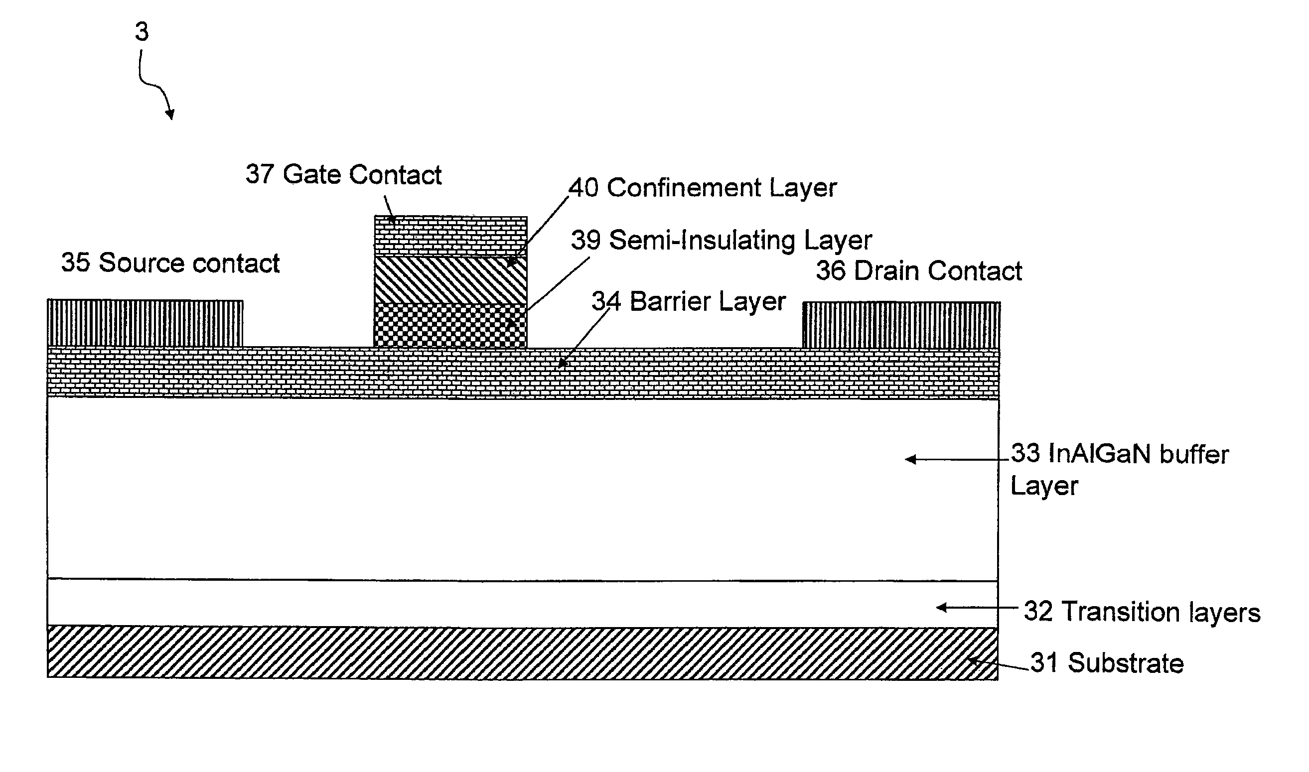
[0031]FIG. 10 shows a GaN transistor 2 according to the present invention. GaN transistor 2 is similar to GaN transistor 1 (FIG. 2), except that GaN transistor 2 has a semi-insulating layer 39 in place of the compensated semiconductor layer 38 (FIG. 2). Semi-insulating layer 39 may comprise, for example, AlGaN or GaN, with deep level impurity atoms, for example, C, Fe, Mn, Cr, V, or Ni. Additionally, a GaN transistor may have both a semi-insulating layer and a compensated semiconductor layer.

[0032]The second embodiment of the invention has the same advantages as the first embodiment. The high doping of semi-insulating layer 39 leads to enhancement mode devices, the semi-insulating layer 39 leads to low gate leakage during device operation, and the insulating nature of semi-insulating 39 reduces the gate capacitance of the device. In addition, the performance of the device of the second embodiment is not as sensitive to future processing steps involving hydrogen and / or high temperatu...

third embodiment

[0036]FIG. 14 shows a GaN transistor 3 according to the present invention. GaN transistor 3 is similar to GaN transistor 2, except that a confinement layer is placed above the semi-insulating layer and below the gate contact layer. This confinement layer can be composed of AlGaN, SiN, SiO2, or other insulating material.

[0037]The method of manufacturing GaN transistor 3 is the same as the method of manufacturing GaN transistor 1 for steps shown in FIGS. 3-6 and GaN transistor 2 for the step shown in FIG. 11. Referring to FIG. 15, the next step is the deposition of an insulating confinement layer 40.

[0038]The third embodiment has the advantage of further reduced gate leakage compared to embodiment 1 or embodiment 2. The disadvantage is a further reduction in conductivity when the device is turned on by applying a positive voltage to the gate contact. A unique advantage of the third embodiment is the creation of a variable threshold voltage device. The confinement layer thickness can b...

fourth embodiment

[0039]FIG. 16 shows a GaN transistor 4 according to the present invention. GaN transistor 4 is similar to GaN transistor 2, except that it has a spacer layer 49 beneath semi-insulating layer 48 and above barrier layer 44. Associated with spacer layer 49, which is a low Mg region, is a doping offset thickness. The low Mg concentration near the barrier layer reduces the back diffusion into the barrier layer.


PUM


Abstract

A MISFET, such as a GaN transistor, with low gate leakage. In one embodiment, the gate leakage is reduced with a compensated GaN layer below the gate contact and above the barrier layer. In another embodiment, the gate leakage is reduced by employing a semi-insulating layer below the gate contact and above the barrier layer.

Description

CROSS REFERENCE TO RELATED APPLICATIONS[0001]This application claims priority from U.S. Provisional Application No. 61 / 167,792 filed on Apr. 8, 2009, which is hereby incorporated by reference in its entirety.FIELD OF THE INVENTION[0002]The present invention relates to the field of enhancement mode gallium nitride (GaN) transistors. More particularly, the invention relates to an enhancement mode GaN transistor with a compensated GaN layer or a semi-insulating GaN layer below the gate contact and above the barrier layer.DETAILED DESCRIPTION OF THE INVENTION[0003]Gallium nitride (GaN) semiconductor devices are increasingly desirable for power semiconductor devices because of their ability to carry large current and support high voltages. Development of these devices has generally been aimed at high power / high frequency applications. Devices fabricated for these types of applications are based on general device structures that exhibit high electron mobility and are referred to variously...

Claims


Application Information

Patent Timeline
Patent Type & Authority Patents(United States)
IPC IPC(8): H01L29/66
CPCH01L29/802H01L29/66522H01L29/2003H01L21/326H01L29/778H01L29/788
Inventor LIDOW, ALEXANDERBEACH, ROBERTCAO, JIANJUNNAKATA, ALANAZHAO, GUANG YUAN
Owner EFFICIENT POWER CONVERSION CORP
Why Eureka
Try Eureka