

Low offset input circuit and transmission system with the input circuit
a low-offset input circuit and input circuit technology, applied in the direction of digital transmission, transmission, amplifier with semiconductor devices/discharge tubes, etc., can solve the problems of increased adjustment time, labor-intensive adjustment, and increased adjustment time, so as to reduce the offset voltage, and detect the offset voltage accurately
- Summary
- Abstract
- Description
- Claims
- Application Information
AI Technical Summary
Benefits of technology
Problems solved by technology
Method used
Image

Examples
first embodiment
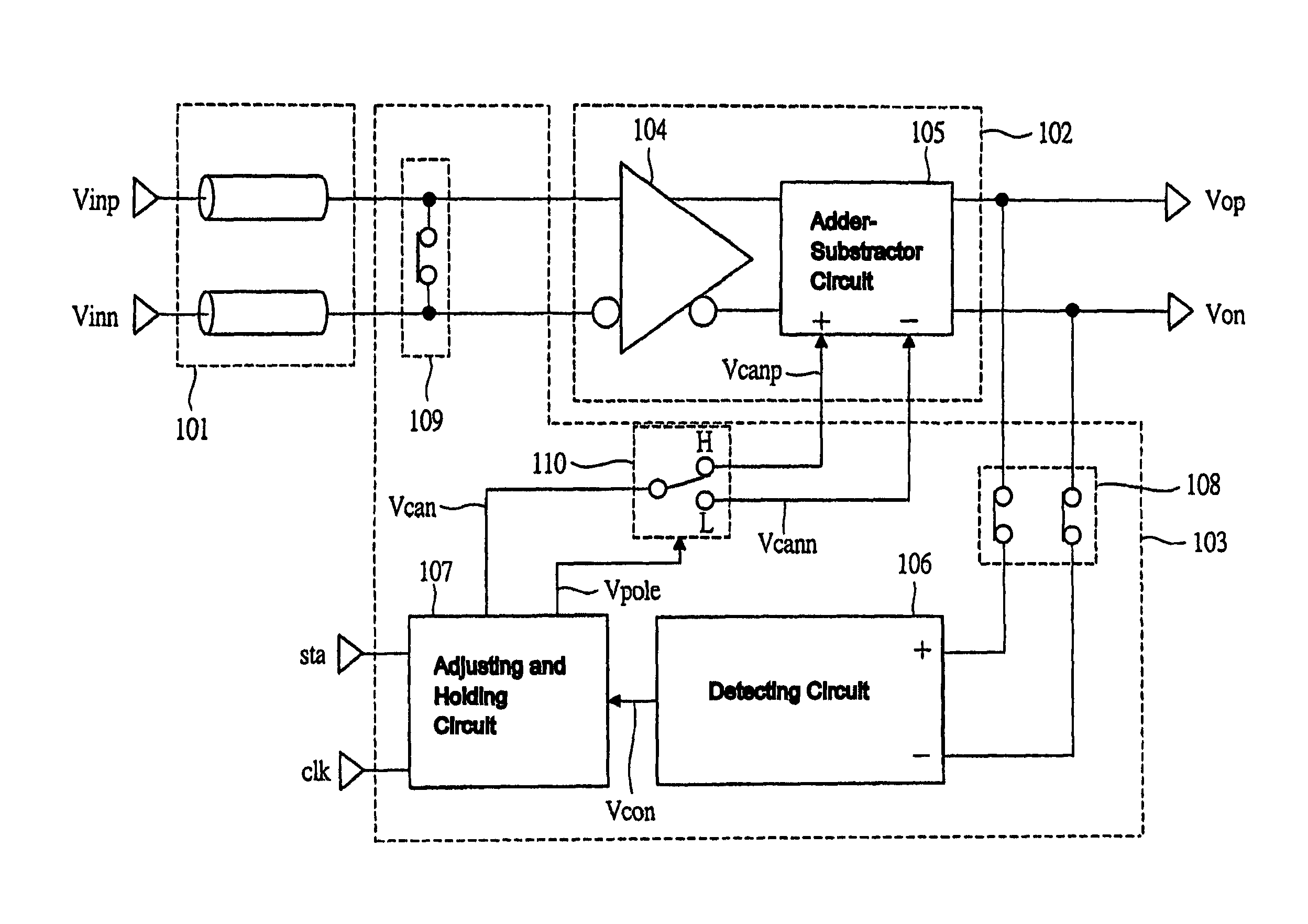
[0037]A low offset input circuit according to a first embodiment cuts off an input circuit from a transmission line by short-circuiting differential input signal terminals of the input circuit; directly detects and holds an offset voltage of the input circuit; and performs negative feedback of the detected amount to the input circuit, thereby reducing the offset voltage of the input circuit. FIG. 1 is a circuit diagram illustrating one example of a configuration of the low offset input circuit according to the first embodiment of the present invention. The low offset input circuit of FIG. 1 has two operation modes of an input circuit offset voltage detecting operation and an input circuit normal operation, and includes an input circuit block 102 which receives a signal from a transmission line 101, and an offset voltage compensating circuit block 103 which reduces an offset voltage of the input circuit block. The input circuit block 102 includes an input circuit 104 which can perfor...
second embodiment
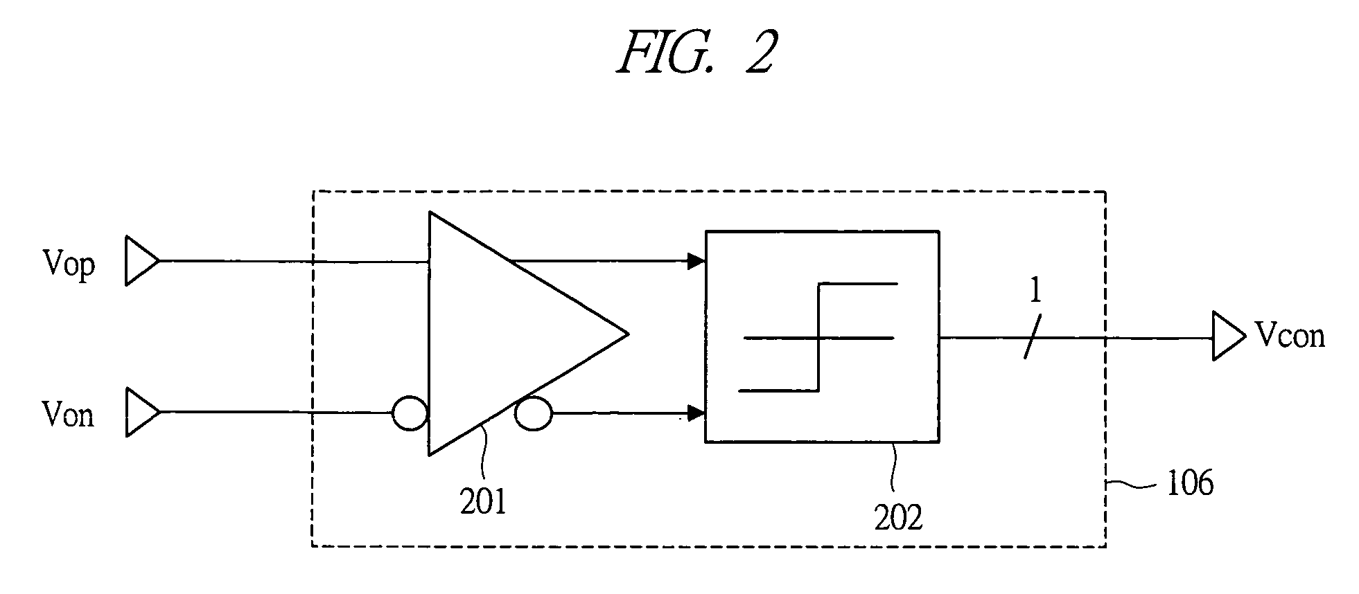
[0040]FIG. 2 is a circuit diagram illustrating one example of a configuration of the detecting circuit block 106 illustrated in FIG. 1 in a low offset input circuit according to a second embodiment of the present invention. The detecting circuit block 106 illustrated in FIG. 2 includes a differential amplifier 201 for a low offset voltage, and a comparator 202. In the present embodiment, variation compensation of the detecting circuit block 106 itself is performed by amplifying an output offset voltage of the input circuit 104 of FIG. 1 in the differential amplifier 201 of a low offset voltage, so that high-precision detection of the offset voltage is made possible. That is, when there is a variation (offset) in the detecting circuit block 106 itself, it is difficult to reduce an output offset voltage of the input circuit 104 with high precision, but such a problem can be solved by using an amplifier having a low offset voltage specification to the differential amplifier 201 in this...
third embodiment
[0042]FIG. 3 is a circuit diagram illustrating a detailed configuration example of the differential amplifier 201 of FIG. 2 in a low offset input circuit according to a third embodiment of the present invention. The differential amplifier 201 illustrated in FIG. 2 is one called “Auto-Zero amplifier” or the like, for example. The Auto-Zero amplifier is a low offset input circuit utilizing sampling, has two operation modes of an auto-zeroing operation and a normal amplifying operation, and includes a high-gain amplifier 301, a sampling capacitor 304, an adder 305, and switches 302 and 303 for selecting one from the abovementioned two operation modes. In the auto-zeroing operation mode, respective switches in FIG. 3 are closed to “L” sides so that an offset voltage of the amplifier 301 is accumulated in the sampling capacitor 304. In the normal amplifying operation, the respective switches are closed to “H” sides, and an input offset voltage accumulated in the sampling capacitor 304 is...
PUM
 Abstract
Description
Claims
Application Information