Method for tuning the work function of a metal gate of the PMOS device

a technology of pmos device and work function, which is applied in the direction of pmos device, basic electric elements, electrical apparatus, etc., can solve the problems of difficult to achieve the high work function required by pmos device, and achieve the effect of rapid thermal annealing, suitable low threshold voltage, and simple and convenient process

Active Publication Date: 2013-02-05
INST OF MICROELECTRONICS CHINESE ACAD OF SCI
View PDF5 Cites 8 Cited by
  • Summary
  • Abstract
  • Description
  • Claims
  • Application Information

AI Technical Summary

Benefits of technology

[0009]Suitable work function can be obtained by optimizing the energy and dose of ion implantation and heat treatment conditions so as to achieve a suitable threshold voltage. The inventive method can be widely used and its process is simple and convenient, as well as has a better ability to tune the work function of the metal gate, and is compatible with the conventional CMOS process.
[0021]The inventive method tunes the work function of a metal gate by doping the metal gate with metal ions and performing rapid thermal annealing so that the doped metal ions accumulate at the interface between the high-k gate dielectric and interfacial SiO2 or generate dipoles by interfacial reaction, and achieves a suitable low threshold voltage. The inventive method can be implemented in a simple and convenient process, has good thermal stability and has a better ability of tuning the work function of the metal gate. Also, the inventive method is compatible with the CMOS process, and can be applied to integrated circuit industry.

Problems solved by technology

However, there are still some urgent problems in integrating the metal gate with the high-k gate dielectric, such as poor thermal stability, unfavorable interface states, and especially the Fermi level pinning effect which makes the challenging to provide an appropriate low threshold voltage required by nanoscale CMOS devices, in particular, for PMOS devices, because it is more difficult to achieve the high work function required by PMOS devices.

Method used


Image

  • Method for tuning the work function of a metal gate of the PMOS device
  • Method for tuning the work function of a metal gate of the PMOS device
  • Method for tuning the work function of a metal gate of the PMOS device

Examples


Embodiment Construction

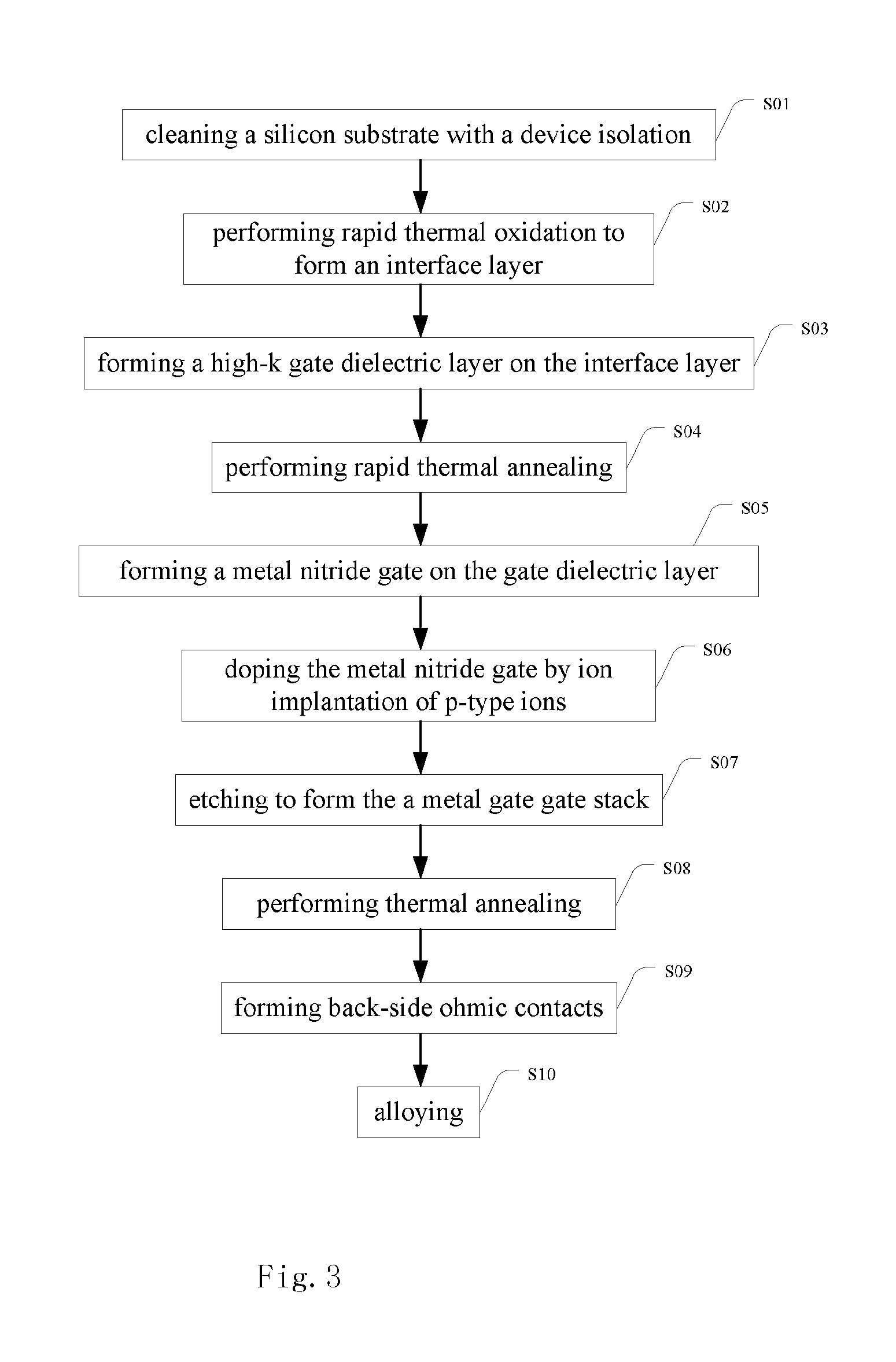
[0025]Step 1: after formation of a device isolation and before formation of an interface oxide layer, cleaning a silicon substrate with device isolation having being formed therein, by firstly washing it with a conventional process, and then immersing it into a mixed solution (hydrofluoric acid:isopropanol:water=0.3-0.8%:0.01-0.08%:1%, by volume) at room temperature for 2-10 minutes, and then rinsing it with deionized water, and then drying it in N2 gas, and then immediately growing interface layer of SiOx (step S01 in FIG. 3);

[0026]Step 2: forming an interface layer of SiOx having a thickness of about 5-7 Å, by using rapid thermal annealing (RTA) in N2 gas for about 20-120 seconds (step S02 in FIG. 3);

[0027]Step 3: forming a high-k gate dielectric layer of HfLaON having a thickness of about 10-40 Å by physical vapor deposition, wherein a Hf—La target and a Hf target are sputtered alternatively in N2 / Ar mixed gas in a magnetron reactive sputtering process, under an working pressure ...


PUM

PropertyMeasurementUnit
thicknessaaaaaaaaaa
thicknessaaaaaaaaaa
RF poweraaaaaaaaaa

Abstract

A method for tuning the work function of a metal gate of the PMOS device is disclosed. The method comprises depositing a layer of metal nitride or a metal on a layer of high-k gate dielectric by physical vapor deposition (PVD), as a metal gate; doping the metal gate with dopants such as Al, Pt, Ru, Ga, Ir by ion implantation; and driving the doped metal ions to the interface between the high-k gate dielectric and interfacial SiO2 by high-temperature annealing so that the doped metal ions accumulate at the interface or generate dipoles by interfacial reaction, which in turn tunes the work function of the metal gate. The method can be widely used and its process is simple and convenient, has a better ability of tuning the work function of the metal gate, and is compatible with the conventional CMOS process.

Description

CROSS-REFERENCE TO RELATED APPLICATION[0001]This Application is a Section 371 National Stage Application of International Application No. PCT / CN2010 / 074596, filed Jun. 28, 2010, not yet published, the contents of which are hereby incorporated by reference in their entirety.BACKGROUND OF THE INVENTION[0002]1. Field of Invention[0003]The present invention relates to semiconductor technology, and in particular, to a method for tuning the work function of a metal gate of the PMOS device, which can be used in manufacture of high performance nanoscale complementary Metal-Oxide-Semiconductor Transistor (CMOS) device at 45 nm and beyond.[0004]2. Description of Prior Art[0005]As a feature size of CMOS device reaches the technology node of 45 nm and beyond, it is well known in the art that the structure of high-k (i. e. dielectric constant) / metal gate materials will be used to replace the conventional structure of SiO2 / poly-Si for remarkably decreasing the gate tunneling current and the gate ...

Claims


Application Information

Patent Timeline
Patent Type & Authority Patents(United States)
IPC IPC(8): H01L21/469
CPCH01L21/28088H01L21/28176H01L21/3215H01L29/4966H01L29/513H01L29/517H01L21/28202H01L21/32136H01L21/823828H01L21/823842
Inventor XU, QIUXIAXU, GAOBO
Owner INST OF MICROELECTRONICS CHINESE ACAD OF SCI
Why Eureka
Try Eureka