Semiconductor memory cell and manufacturing method thereof, and semiconductor memory devices

Inactive Publication Date: 2013-02-26
PANASONIC CORP
View PDF31 Cites 8 Cited by
  • Summary
  • Abstract
  • Description
  • Claims
  • Application Information

AI Technical Summary

Benefits of technology

[0014]A semiconductor memory cell according to the present invention includes: a memory element formed by a first field effect transistor having a gate insulating film made of a ferroelectric film; and a select switching element formed by a second field effect transistor having a gate insulating film made of a paraelectric film, wherein the ferroelectric film and the paraelectric film are stacked together with a semiconductor film of a compound semiconductor interposed therebetween, a first gate electrode of the first field effect transistor is formed on a side of the ferroelectric film, a second gate electrode of the second field effect transistor is formed on a side of the paraelectric film so as to face the first gate electrode, and the semiconductor film forms a common channel layer of the first and second field effect transistors.
[0015]With the above configuration, resistance of the semiconductor film that forms the common channel layer of the first and second field effect transistors can be independently controlled by a polarization state of the ferroelectric film (data written in the memory element) and a voltage that is applied to the second gate electrode (an operating voltage of the select switching element). Thus, in a NAND-type semiconductor memory device having multiple ones of the semiconductor memory cells of the present invention connected in series, read operation and write operation can be performed by simple control.
[0016]Since the compound semiconductor film is used as the semiconductor film, carriers in the

Problems solved by technology

However, increasing the thickness of the semiconductor film reduces the quality of the semiconductor film, thereby bringing new problems such as reducing reliability and making it difficult to form the source/drain regions by ion implantation.
How

Method used


Image

  • Semiconductor memory cell and manufacturing method thereof, and semiconductor memory devices
  • Semiconductor memory cell and manufacturing method thereof, and semiconductor memory devices
  • Semiconductor memory cell and manufacturing method thereof, and semiconductor memory devices

Examples


Example

[0048](First Embodiment)

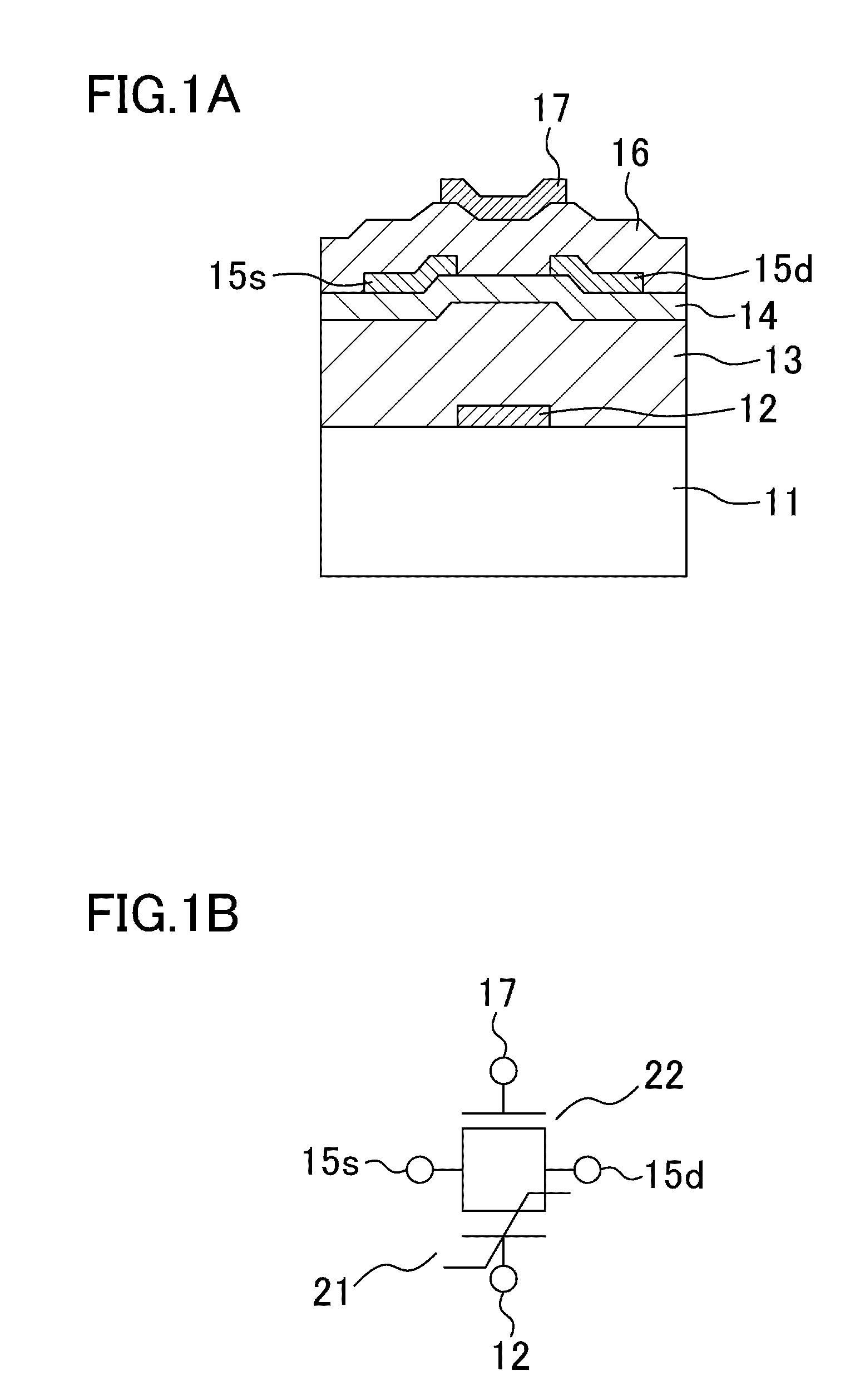
[0049]FIGS. 1A-1B are diagrams schematically showing a configuration of a semiconductor memory cell in a first embodiment of the present invention, where FIG. 1A is a cross-sectional view of the semiconductor memory cell, and FIG. 1B is an equivalent circuit diagram thereof.

[0050]As shown in FIG. 1A, a ferroelectric film 13 and a paraelectric film 16 are stacked together over a substrate 11 with a semiconductor film 14 interposed between the ferroelectric film 13 and the paraelectric film 16. A first gate electrode 12 of a first field effect transistor (FET) is formed on the side of the ferroelectric film 13, and a second gate electrode 17 of a second FET is formed on the side of the paraelectric film 16 so as to face the first gate electrode 12. The semiconductor film 14 is made of a compound semiconductor that forms a common channel layer of the first and second FETs, and a common source electrode 15s and a common drain electrode 15d of the first and second...

Example

[0090](Second Embodiment)

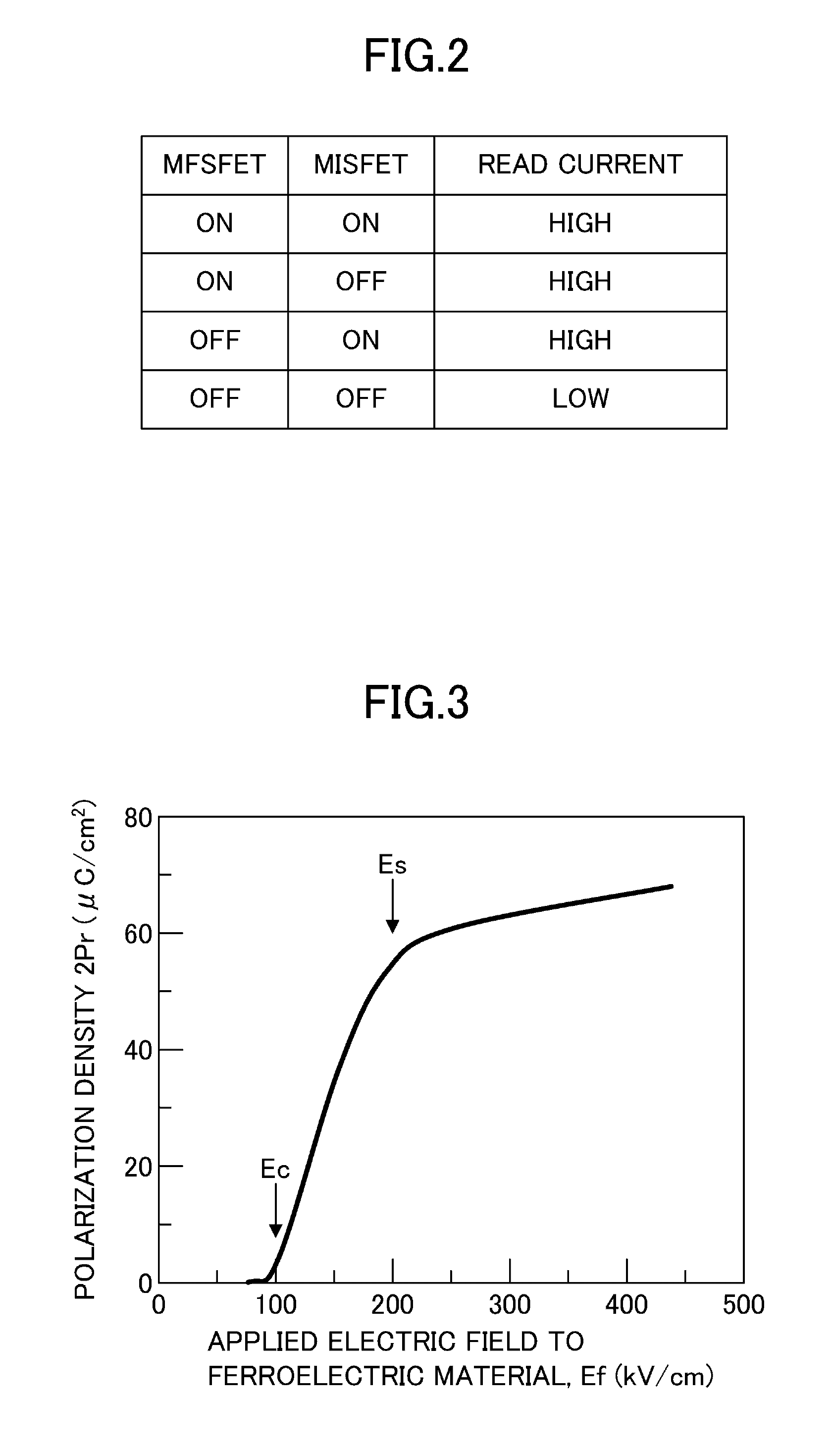
[0091]In the NAND-type nonvolatile memory described in Patent Document 2, data written to a selected memory cell is read by turning off only the MISFET of this memory cell and turning on the other MISFETs, and measuring a current flowing in a memory block where the memory cells are connected in series.

[0092]Since FETs having a gate insulating film of a paraelectric material are used as the MISFETs of these memory cells, these MISFETs are also used for select transistors of the memory block. Thus, these MISFETs are usually of a normally-off type. When reading the nonvolatile memory using the normally-off type transistors, a voltage is applied to the gate electrodes in order to turn on the MISFETs of the non-selected memory cells. As a result, the polarization state of the ferroelectric film of the non-selected memory cells is reversed, which may disturb the data written in the memory cell.

[0093]When reading the nonvolatile memory, a predetermined voltage need...

Example

[0119](Third Embodiment)

[0120]The semiconductor memory device that does not cause disturbance in read operation of the semiconductor memory cells is described in the second embodiment. A semiconductor memory device that does not cause disturbance in write operation to semiconductor memory cells will be described in a third embodiment of the present invention.

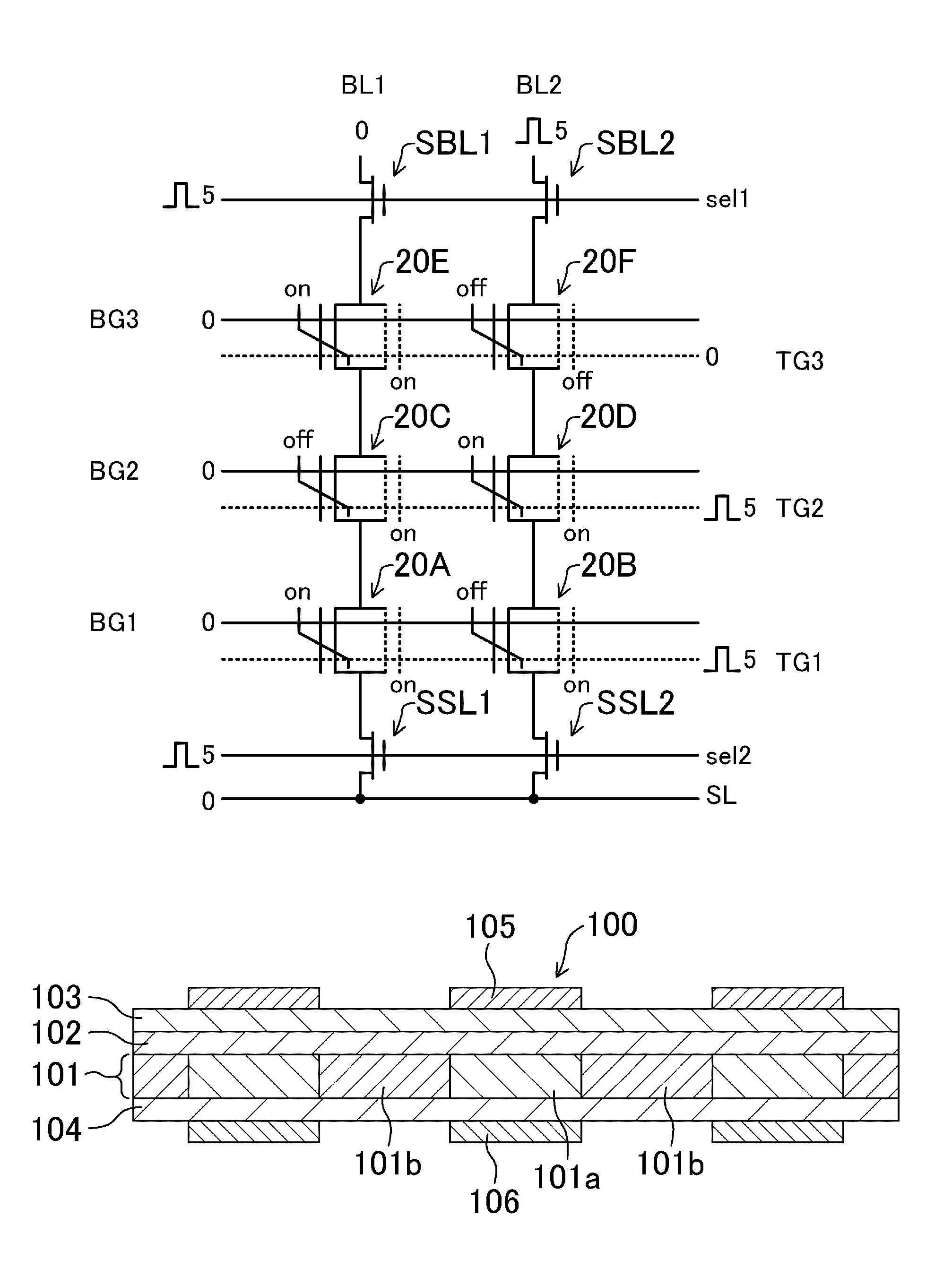
[0121]Write operation to the semiconductor memory cells (hereinafter simply referred to as the “memory cells”) arranged in an array will be described with reference to FIGS. 19A-22B. An example will be described in which memory cells 20A-20F are arranged in three rows by two columns. MISFETs forming select switching elements of the memory cells are of a normally-on type.

[0122]First, reset operation that is performed before write operation will be described with reference to FIGS. 19A-19B. FIG. 19A is a circuit diagram showing a memory cell layout, and FIG. 19B is a timing chart of the reset operation.

[0123]As shown in FIG. 19A, ...


PUM


Abstract

A semiconductor memory cell includes: a memory element formed by a first field effect transistor having a gate insulating film made of a ferroelectric film; and a select switching element formed by a second field effect transistor having a gate insulating film made of a paraelectric film. The ferroelectric film and the paraelectric film are stacked together with a semiconductor film of a compound semiconductor interposed therebetween. A first gate electrode of the first field effect transistor is formed on a side of the ferroelectric film, and a second gate electrode of the second field effect transistor is formed on a side of the paraelectric film so as to face the first gate electrode. The semiconductor film forms a common channel layer of the first and second field effect transistors.

Description

CROSS-REFERENCE TO RELATED APPLICATION[0001]This is a continuation of PCT International Application PCT / JP2009 / 005595 filed on Oct. 23, 2009, which claims priority to Japanese Patent Application No. 2009-040878 filed on Feb. 24, 2009, Japanese Patent Application No. 2009-054919 filed on Mar. 9, 2009, and Japanese Patent Application No. 2009-119619 filed on May 18, 2009. The disclosures of these applications including the specifications, the drawings, and the claims are hereby incorporated by reference in their entirety.BACKGROUND[0002]The present invention relates to semiconductor memory cells including a memory element formed by a field effect transistor having a gate insulating film made of a ferroelectric film, and semiconductor memory devices having semiconductor memory cells arranged in an array.[0003]Nonvolatile memories using a ferroelectric material are roughly divided into two types, namely a capacitor type and a field effect transistor (FET) type having a gate insulating f...

Claims


Application Information

Patent Timeline
IPC IPC(8): G11C11/22
CPCG11C11/22H01L21/28291H01L29/78391H01L29/516H01L29/6684H01L27/1159G11C11/223H01L29/40111H10B51/30
Inventor KANEKO, YUKIHIROKATO, YOSHIHISATANAKA, HIROYUKI
Owner PANASONIC CORP
Why Eureka
Try Eureka