Sapphire substrate, nitride semiconductor luminescent element using the sapphire substrate, and method for manufacturing the nitride semiconductor luminescent element

a technology of nitride semiconductor and substrate, which is applied in the direction of polycrystalline material growth, crystal growth process, chemically reactive gas growth, etc., can solve the problems of m-plane gan not growing, cumbersome and complicated process of related art, and high cost of sic or lialo/sub>substrates, etc., to improve radiative recombination efficiency, reduce the influence of piezo electric fields, and increase the overlap of wave functions

Active Publication Date: 2013-03-05
PANASONIC CORP
View PDF16 Cites 14 Cited by
  • Summary
  • Abstract
  • Description
  • Claims
  • Application Information

AI Technical Summary

Benefits of technology

[0008]A method for manufacturing a sapphire substrate, a nitride semiconductor luminescent element using the sapphire substrate, and a nitride semiconductor luminescent element in accordance with the present invention uses the sapphire substrate for crystal growth and include a cutting step of preparing a-plane slanted from the m-plane by a predetermined very small angle, prior to a crystal growth step, at the time of using the m-plane of the sapphire substrate as a growth surface. With the manufacturing method configured in this way, a c-plane of GaN is allowed to grow from each step plane formed as an a-plane onto a terrace in a vapor phase method, such as an MOCVD method, by controlling the steps of a substrate, even if an inexpensive sapphire substrate which normally does not form any m-plane (nonpolar plane) GaN film is used as the substrate for crystal growth. Thus, an epitaxially-grown excellent GaN single crystal continues to grow, so that the m-plane thereof is opposite to the surplane of the terrace. In the mean time, the respective steps become integrated (fused) with one another. Thus, it is possible to grow an m-plane GaN single crystal. In addition, the use of an m-plane eliminates the influence of piezo electric fields and makes it possible to increase the overlap of wave functions between electrons and holes. In this way, a substrate and a device which can enhance radiative recombination efficiency, i.e., internal quantum efficiency, can be realized.

Problems solved by technology

Until now, however, an extremely expensive SiC or LiAlO2 substrate, for example, has been necessary for the luminescence of GaN in the m-plane.
Thus, the process of the related art is cumbersome and complicated, compared with a vapor phase method in which a process from the fabrication of a substrate to the fabrication of a device can be carried out continuously.
In that method, however, m-plane GaN does not grow and only semipolar GaN is obtained.

Method used


Image

  • Sapphire substrate, nitride semiconductor luminescent element using the sapphire substrate, and method for manufacturing the nitride semiconductor luminescent element
  • Sapphire substrate, nitride semiconductor luminescent element using the sapphire substrate, and method for manufacturing the nitride semiconductor luminescent element
  • Sapphire substrate, nitride semiconductor luminescent element using the sapphire substrate, and method for manufacturing the nitride semiconductor luminescent element

Examples


Embodiment Construction

[0014]Hereinafter, one embodiment in accordance with the present invention will be described on the basis of the accompanying drawings. Note that in the respective drawings, constituent elements denoted by like reference numerals are the same as one another and will not be explained again.

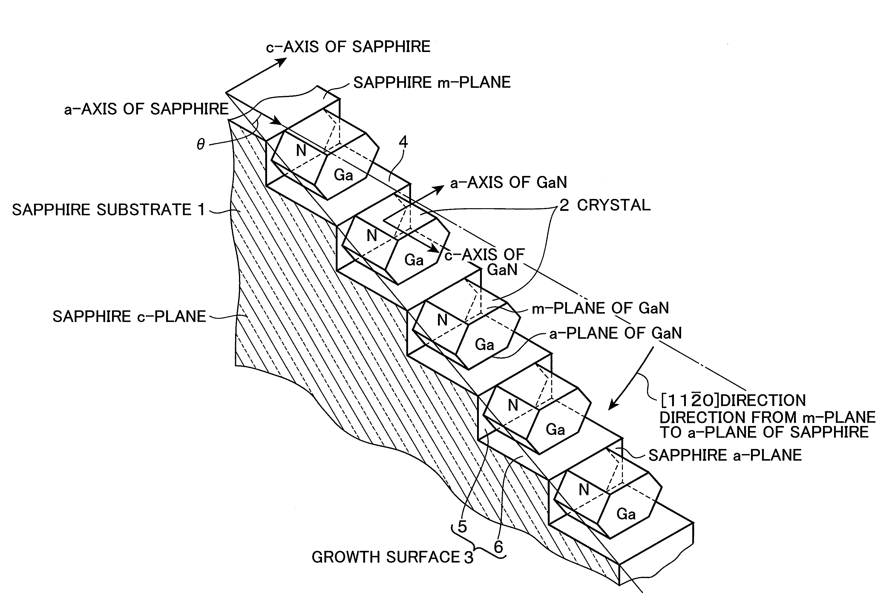
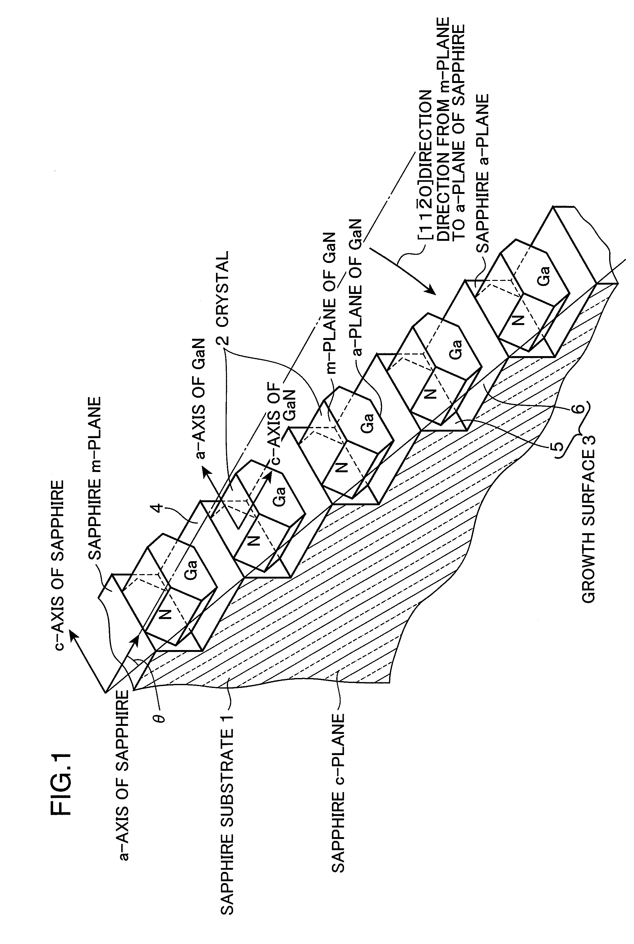
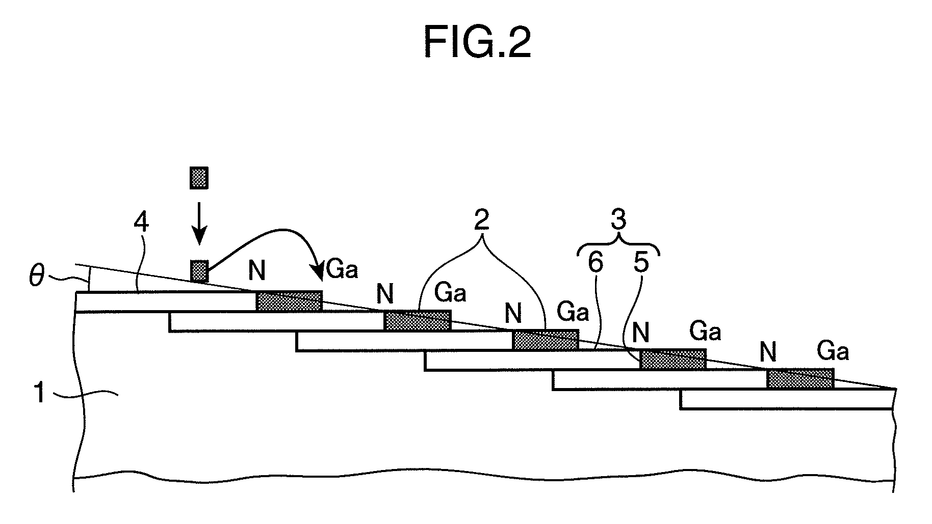
[0015]FIG. 1 is a perspective view illustrating the growth process of a nitride semiconductor luminescent element using a sapphire substrate 1 in accordance with one embodiment of the present invention, whereas FIG. 2 is a vertical cross-sectional view of FIG. 1. It should be noted that in the sapphire substrate 1 of the present embodiment, when a crystal 2 which is a nitride semiconductor of a III-V group or the like, such as GaN, is grown, there is first prepared by a cutting step, an off-angle plane, as a growth surface 3 to serve as a template of the crystal 2, slanted from an m-plane 4 by a predetermined very small angle θ, preferably 0.2 to 10 degrees, more preferably 0.5 to 4 degrees, and pa...


PUM

PropertyMeasurementUnit
angleaaaaaaaaaa
heightaaaaaaaaaa
heightaaaaaaaaaa

Abstract

The present invention provides an inexpensive substrate which can realize m-plane growth of a crystal by vapor phase growth. In a sapphire substrate, an off-angle plane slanted from an m-plane by a predetermined very small angle is prepared as a growth surface, which is a template of the crystal, at the time of growing a crystal of GaN or the like, by a polishing process to prepare a stepwise substrate comprising steps and terraces. According to the above-described configuration, even if an inexpensive sapphire substrate, which normally does not form an m-plane (nonpolar plane) GaN film, is used as a substrate for crystal growth, the following advantages can be attained. Specifically, c-axis growth can be carried out from the plane of each step as an a-plane on the terrace by vapor phase growth, which is advantageous in the fabrication of a device, in order to grow an excellent GaN single crystal which has been epitaxially grown so that the m-plane is opposite to the surplane of the terrace, and, in the mean time, the steps become integrated (fused), whereby a device can be fabricated from a substrate of a GaN single crystal having no significant threading dislocation. Further, the use of the m-plane can advantageously eliminate the influence of piezo electric fields.

Description

TECHNICAL FIELD[0001]The present invention relates to a sapphire substrate, a nitride semiconductor luminescent element using the sapphire substrate, and a method for manufacturing the nitride semiconductor luminescent element.BACKGROUND ART[0002]In recent years, a nitride semiconductor luminescent element having an emission layer composed of a III-V group nitride semiconductor or the like has been a focus of attention. In one example, the structure of this luminescent element is composed in the manner that a sapphire substrate is used and there are formed, respectively, an emission layer made of InGaN or the like, a contact layer made of an n+-GaN layer doped with silicon (Si) on the lower portion of the emission layer, an electron blocking layer made of p-AlxGa1-xN doped with magnesium (Mg) on the upper portion of the emission layer, and a contact layer made of p-GaN on the upper portion of the electron blocking layer.[0003]At present, such a GaN device as described above is forme...

Claims


Application Information

Patent Timeline
Patent Type & Authority Patents(United States)
IPC IPC(8): H01L33/00H01L33/16
CPCC30B25/02C30B25/18C30B29/403C30B29/406H01L21/0242H01L21/0243H01L21/02433H01L21/02458H01L21/0254H01L21/02609H01L21/02661H01L33/007H01L33/16
Inventor ARMITAGE, ROBERT DAVIDKONDO, YUKIHIROHIRAYAMA, HIDEKI
Owner PANASONIC CORP
Why Eureka
Try Eureka