Pattern check device and pattern check method

a technology of pattern check and pattern, which is applied in the direction of semiconductor/solid-state device testing/measurement, instruments, and operators, can solve the problems of reducing the reliability of inspection, reducing and doubting whether it indicates the real charge state, so as to prevent the sensitivity of defect detection from being reduced, stable inspection, and preventing the effect of reliability reduction

Active Publication Date: 2013-04-16
HITACHI HIGH-TECH CORP
View PDF16 Cites 5 Cited by
  • Summary
  • Abstract
  • Description
  • Claims
  • Application Information

AI Technical Summary

Benefits of technology

[0014]The above-described configuration permits a pattern inspection apparatus to simply set an optimal condition of precharge with respect to a pattern, prevent sensitivity for a defect detection from being reduced, automatically inspection whether the precharge is good or not, feed inspection results back to an operation afterward, prevent reliability of them from being reduced, and always perform a stable inspection.

Problems solved by technology

Even if a desired image is obtained by repeating the above, the operator has a defect of requiring much time until final setting of the precharge conditions.
As described above, the inspection apparatus plays a role in monitoring the presence or absence of defects in a semiconductor manufacturing line; however, when the precharge is not appropriate, reliability of the inspection is lowered.
However, with regard to the method for previously obtaining a relationship between the image and the charged state, and then estimating the charge amount from the image acquired prior to an inspection, it is doubtful whether it indicates its real charged state.

Method used


Image

  • Pattern check device and pattern check method
  • Pattern check device and pattern check method
  • Pattern check device and pattern check method

Examples


Embodiment Construction

[0029]Preferred embodiments of the present invention will be described below with reference to the accompanying drawings.

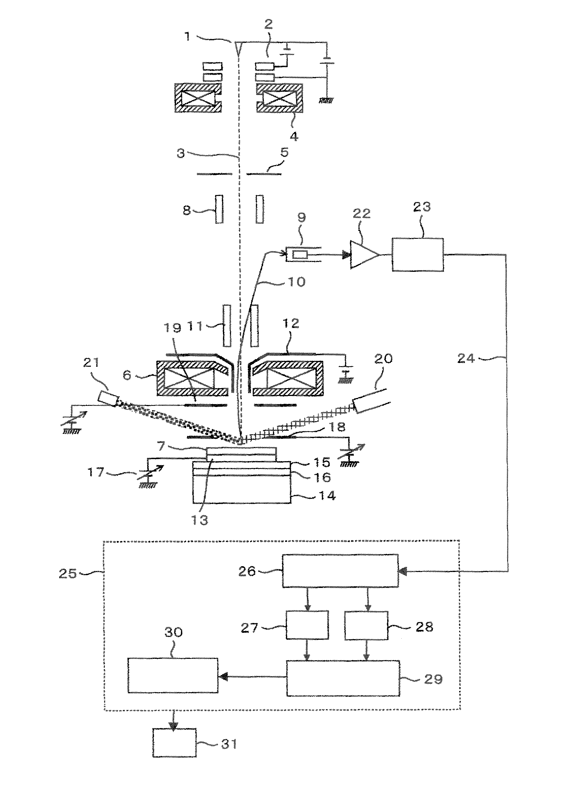
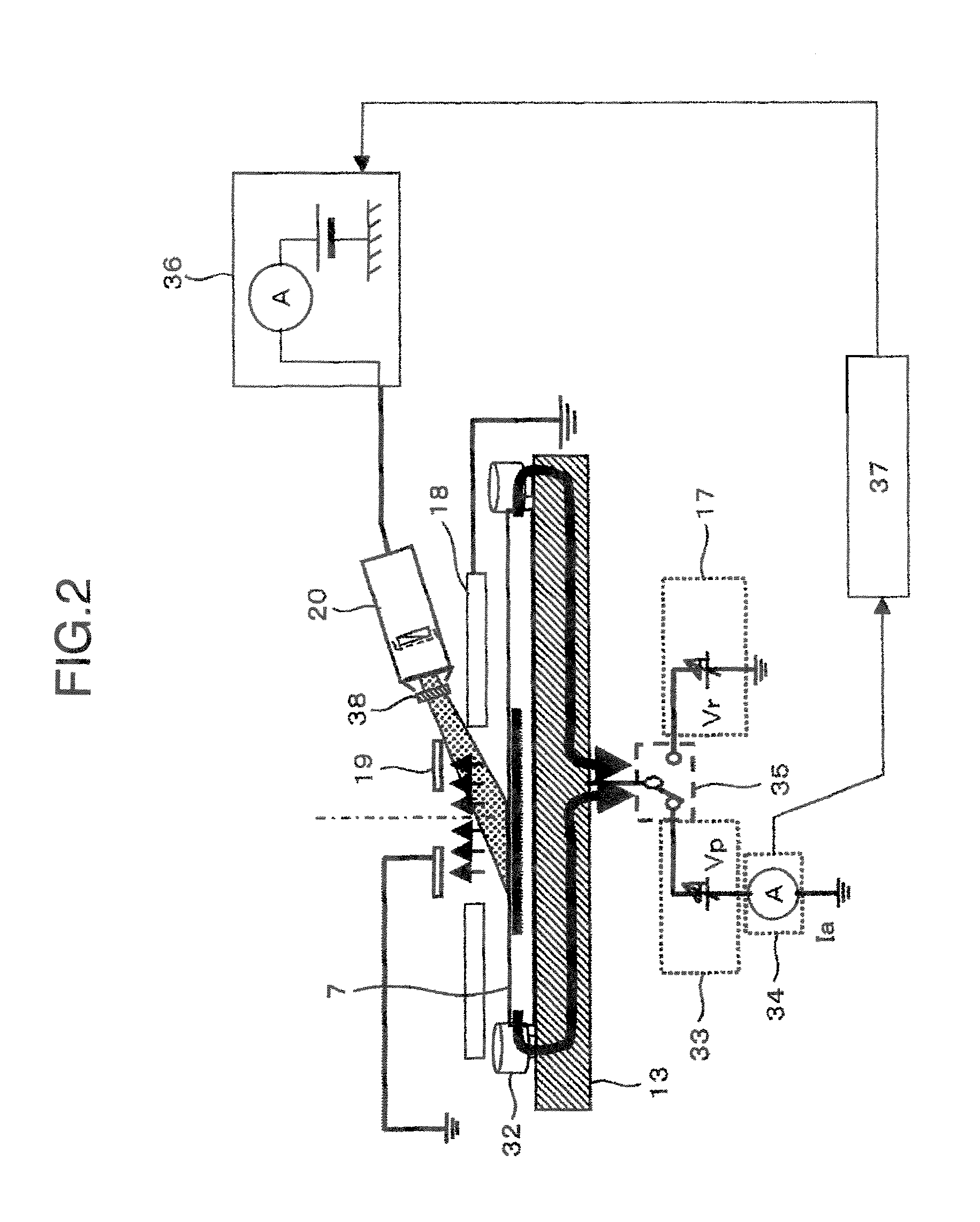
[0030]A pattern inspection apparatus according to the present embodiment of the invention is a circuit pattern inspection apparatus including means which irradiates an electron beam onto a surface of a substrate on which the circuit pattern is formed, means which detects a signal generated from the substrate, and means which images a signal detected by the detection means, and further includes means which forms a charge by another electron source as a preprocessing of an inspection, means which adjusts the charge amount, means which measures the charge amount, means which registers the charge adjustment amount as an inspection condition, means which compares the registration condition and the measurement charge amount, means which inspections based on the comparison whether or not the charge amount becomes equal to a desired value, and means which determines, base...


PUM

PropertyMeasurementUnit
currentaaaaaaaaaa
current measuringaaaaaaaaaa
emission currentaaaaaaaaaa

Abstract

Provided is a pattern inspection apparatus including: a charge formation means which forms charge on a surface of a substrate (7) by generating an electron beam from a second electron source (20) which is different from an electron source (1) which generates an electron beam before irradiating an electron beam (3), a current measuring means (34) which measures a value of current flowing in the substrate while the charge is formed on the surface of the substrate by the charge formation means; and an adjustment means (37) which adjusts the charge formed by the charge formation means so that the value of the current measured by the current measuring means is a predetermined target value. Provided is also a pattern inspection method which uses the pattern inspection apparatus. Thus, it is possible to easily set an optimal condition of precharge executed before inspection of a pattern formed by a semiconductor apparatus manufacturing process and automatically inspection whether the precharge is good. Then, the inspection result is fed back to the operation afterward. This prevents lowering of the reliability of the inspection result and always enables a stable inspection.

Description

RELATED APPLICATIONS[0001]This application is the U.S. National Phase under 35 U.S.C. §371 of International Application No. PCT / JP2009 / 005372, filed on Oct. 15, 2009, which in turn claims the benefit of Japanese Application No. 2008-291624, filed on Nov. 14, 2008, the disclosures of which Applications are incorporated by reference herein.TECHNICAL FIELD[0002]The present invention relates to a technique for inspecting a fine pattern in the middle of a manufacturing process of a semiconductor apparatus and a photomask.BACKGROUND ART[0003]As a sample to be inspected, an inspection of a semiconductor wafer will be described as one example. A process in which a pattern formed on a photomask on a semiconductor wafer is transferred by a lithographic processing and an etching processing is repeated to thereby manufacture a semiconductor apparatus. In a manufacturing process of the semiconductor apparatus, the lithographic processing, the etching processing, quality of other various processi...

Claims


Application Information

Patent Timeline
Patent Type & Authority Patents(United States)
IPC IPC(8): H01J37/26H01J37/304G01N23/00
CPCH01J37/244H01J37/28H01L22/12H01L22/20H01J2237/0048H01J2237/2008H01J2237/24564H01J2237/2817H01L2924/0002H01L2924/00
Inventor NOZOE, MARIMIYAI, HIROSHIOKAMURA, MITSURUSUZUKI, MAKOTOOMINAMI, YUSUKE
Owner HITACHI HIGH-TECH CORP
Why Eureka
Try Eureka